Method of forming interconnection in semiconductor device

a technology of interconnection and semiconductor, applied in the direction of semiconductor/solid-state device manufacturing, basic electric elements, electric devices, etc., can solve the problems of excessive film thickness and stress change, difficult to solve, etc., and achieve the effect of suppressing the impact of uv curing, high uv absorption rate, and greater extinction coefficien

Active Publication Date: 2006-07-20
ASM JAPAN
View PDF3 Cites 33 Cited by
  • Summary
  • Abstract
  • Description
  • Claims
  • Application Information

AI Technical Summary

Benefits of technology

[0004] According to one embodiment of the present invention, the above-mentioned problem is solved by selecting a UV blocking film, which absorbs UV light used for UV curing and suppresses the impact of the UV curing on an underlying layer, and by forming the film between each layer of low-k films. As a UV blocking film, a film having a greater extinction coefficient at UV wavelengths used, and a high rate of UV absorption is preferable. By forming a UV blocking film, excessive curing of an underlying low-k film can be prevented and the integrity of the laminated structure can be preserved. In another embodiment of the present invention, by applying UV curing when a laminated structure is formed by Single Damascene and / or Dual Damascene and using a UV blocking film, an elastic modulus (EM), etc. of a low-k film are effectively improved. Additionally, in still another embodiment, a UV blocking film and an etch stop film are formed separately; in an embodiment, a single film is used both as a UV blocking film and an etch stop film. When UV light having wavelengths of 200 nm or less is used, using a film having high selectively of UV absorption such as SiC, SiCN, SiCO and SiN as an etch stopper between each layer of low-k films, an impact of UV irradiation on an underlying layer can be suppressed without using a UV blocking film separately.

Problems solved by technology

If an underlying low-k film is cured more than necessary, its film thickness and stress change excessively and separation occurs in a bonding surface of Cu wiring buried in a low-k material and the low-k material.
An amount of shrinkage and an amount of hardening are affected by an irradiation time, irradiation intensity, a substrate temperature and a type of gas in an irradiation atmosphere, and it is difficult to solve the above-mentioned problem by irradiation conditions.

Method used


Image

  • Method of forming interconnection in semiconductor device
  • Method of forming interconnection in semiconductor device
  • Method of forming interconnection in semiconductor device

Examples


examples

[0076] Examples of the present invention are shown below. The present invention, however, is not limited to these.

[0077] Process and Irradiation Conditions

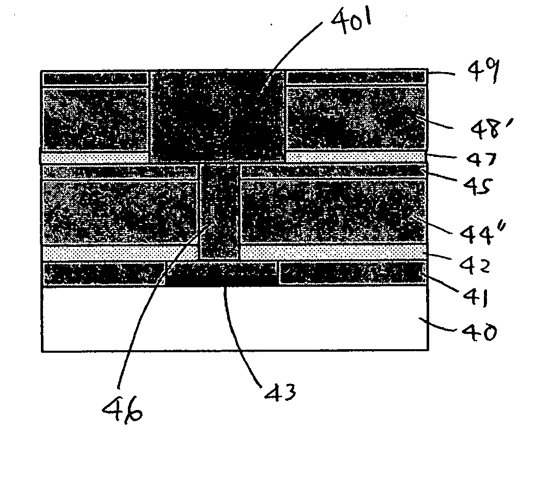
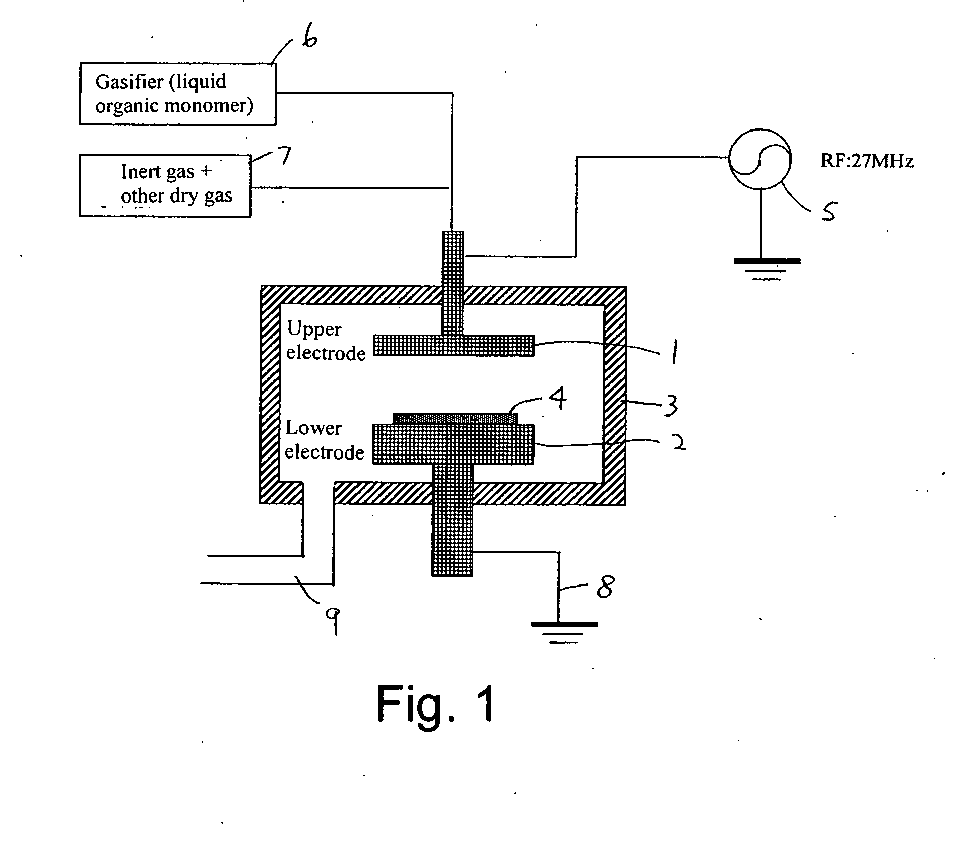
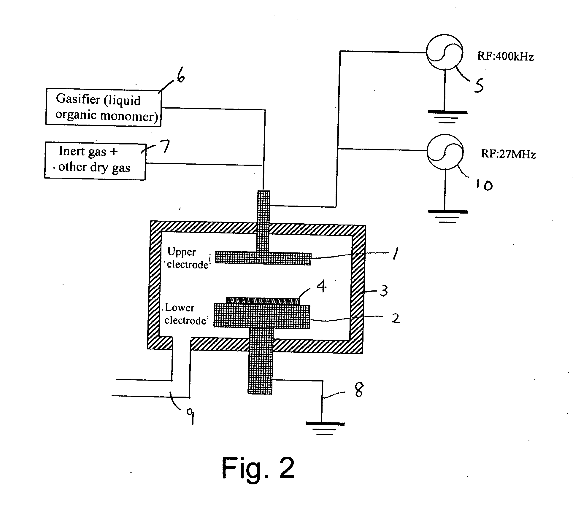
[0078] First, using an apparatus shown in FIG. 1, a low-k film 61 was formed with a thickness of approximately 500 nm on a silicon substrate 61 (300 mm in diameter) using 1,3-dimethoxy-tetramethyldisiloxane (DMOTMDS) as a source gas (FIG. 6A). Additionally, film formation conditions were as follows: 200 scm of DMOTMDS, 100 sccm of O2, 200 sccm of He, RF power of 27.12 MHz at 2.5 W / cm2, a substrate temperature of 360° C. and a pressure of 665 Pa. Next, using the apparatus shown in FIG. 3, UV light was irradiated to the substrate under the conditions described below to reform the low-k film 61 and a reformed low-k film 61′ was obtained (FIG. 6B).

[0079] Processing time: 60 sec.

[0080] UV wavelength: 172 nm

[0081] Irradiation intensity: 10 mW / cm2

[0082] N2: 4,000 sccm

[0083] Pressure: 50 Torr

[0084] Heater temperature: 430° C.

[008...


PUM

PropertyMeasurementUnit
thicknessaaaaaaaaaa
thicknessaaaaaaaaaa
wavelengthaaaaaaaaaa

Abstract

A multilayer interconnection structure is formed by a method comprising the steps of: Forming a low dielectric constant film on a substrate, curing the low dielectric constant film by irradiating it with UV light, laminating a UV blocking film, laminating a next low dielectric constant film, and curing the next low dielectric constant film by irradiating it with UV light.

Description

BACKGROUND OF THE INVENTION [0001] The present invention generally relates to a method of forming an interconnection in a semiconductor device; and more particularly to a method of forming an interconnection by Single Damascene and / or Dual Damascene. [0002] As sizes of wiring design continue to shrink and a wiring structure became multilayered with semiconductor devices getting highly integrated, it is indispensable to lower interlayer capacitance so as to improve high speed of a device and to reduce power consumption. In order to lower the interlayer capacitance, low-k materials (low dielectric constant films) are used. The low-k materials, however, have a very low elastic modulus (EM) of approximately 4-6 GPa in the vicinity of a dielectric constant (k) of 2.5 as compared with conventional TEOS-SiO2 having an elastic modulus of 70-80 GPa; hence, it is difficult for the low-k materials to withstand stress that they receive during a post-process such as CMP, wiring bonding and packa...

Claims


Application Information

Patent Timeline
Patent Type & Authority Applications(United States)
IPC IPC(8): H01L21/4763
CPCH01L21/76801H01L21/76807H01L21/76825
Inventor MATSUSHITA, KIYOHIROOHARA, NAOKIKEMELING, NATHAN R.C.
Owner ASM JAPAN
Why Eureka
Try Eureka