Formation of low K material utilizing process having readily cleaned by-products

a technology of low k material and by-products, which is applied in the direction of coatings, solid-state devices, chemical vapor deposition coatings, etc., can solve the problems of increasing parasitic capacitance between devices, reducing the response time of devices, and damage to device structures

Inactive Publication Date: 2006-07-20
APPLIED MATERIALS INC
View PDF11 Cites 18 Cited by
  • Summary
  • Abstract
  • Description
  • Claims
  • Application Information

AI Technical Summary

Benefits of technology

[0011] Nano-porous low dielectric constant films are deposited utilizing materials having reactive by-products readily removed from a processing chamber by plasma cleaning. In accordance with one embodiment, an oxidizable silicon containing compound is reacted with an oxidizable non-silicon component having thermally labile groups, in a reactive oxygen ambient and in the presence of a plasma. The deposited silicon oxide film is annealed to form dispersed microscopic voids or pores that remain in the nano-porous silicon. Oxidizable non-silicon components with thermally labile groups that leave by-products readily removed from the chamber, include but are not limited to, limonene, carene, cymene, fenchone, vinyl acetate, methyl methacrylate, ethyl vinyl ether, tetrahydrofuran, furan, 2,5-Norbornadiene, cyclopentene, cyclopentene oxide, methyl cyclopentene, 2-cyclopentene-1-one, and 1-butene.

Problems solved by technology

The high temperatures at which some thermal CVD processes operate can damage device structures having layers previously formed on the substrate.
However, the barrier / liner layers typically have dielectric constants that are greater than about 2.5, and the high dielectric constants result in a combined insulator that may not significantly reduce the dielectric constant.
Additionally, the smaller device geometries result in an increase in parasitic capacitance between devices.
Parasitic capacitance between metal interconnects on the same or adjacent layers in the circuit can result in crosstalk between the metal lines or interconnects and / or resistance-capacitance (RC) delay, thereby reducing the response time of the device and degrading the overall performance of the device.
Increasing the thickness of the dielectric materials, however, does not address parasitic capacitance within the same metallized layer or plane.

Method used


Image

  • Formation of low K material utilizing process having readily cleaned by-products
  • Formation of low K material utilizing process having readily cleaned by-products
  • Formation of low K material utilizing process having readily cleaned by-products

Examples


examples

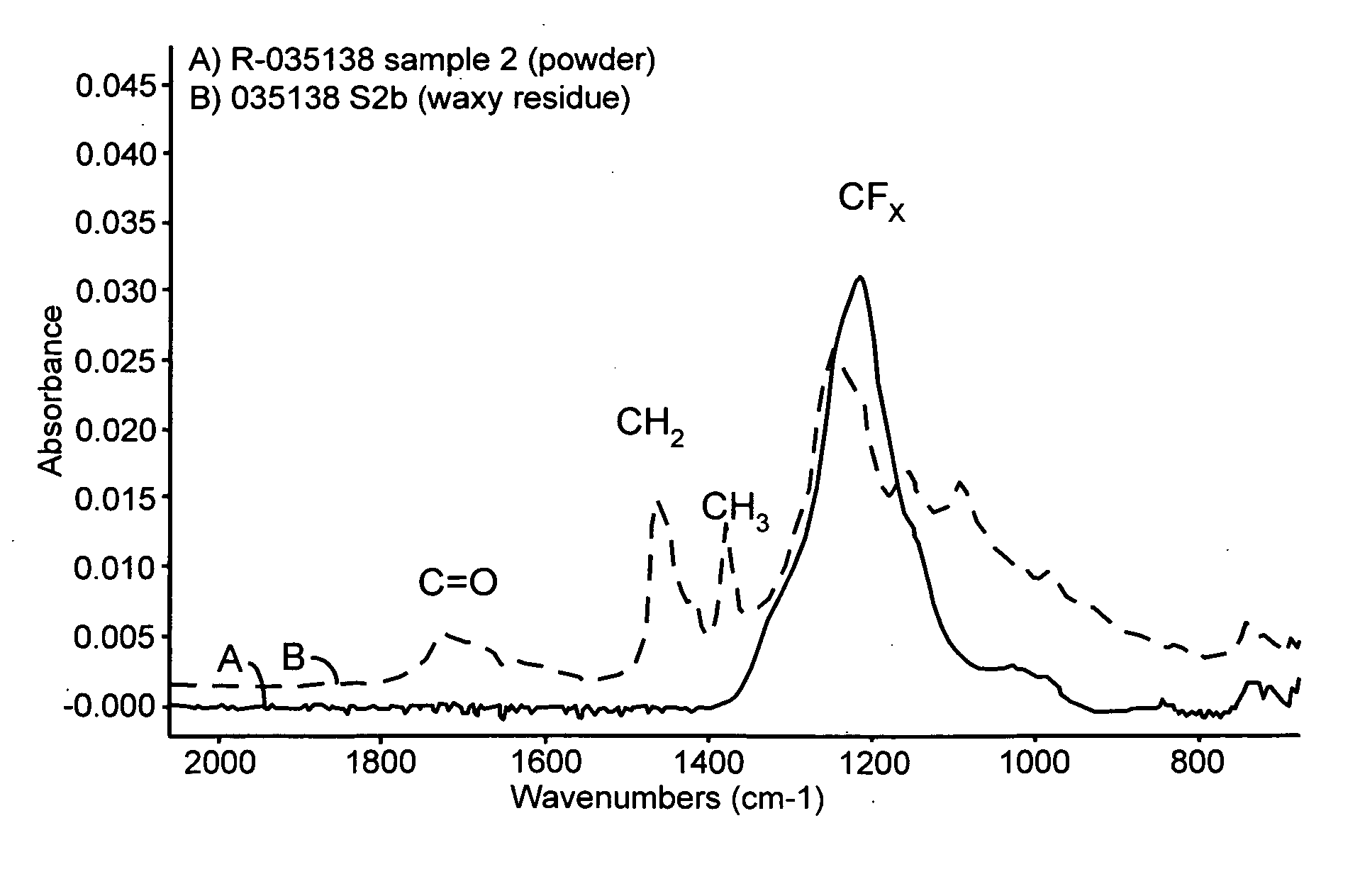
[0097] The following examples demonstrate deposition of a nano-porous silicon oxide based film having dispersed microscopic gas voids. This example is undertaken using a chemical vapor deposition chamber, and in particular, a CENTURA “DLK” system fabricated and sold by Applied Materials, Inc., Santa Clara, Calif.

Silicon Compound Having Silicon Containing and Thermally Labile Imparting Components (Hypothetical)

[0098] A nano-porous silicon oxide based film is deposited at a chamber pressure of 1.0 Torr and temperature of 30° C. from reactive gases which are vaporized and flown into the reactor as follows:

methylsilyl-2-furyl ether, at 150 sccmnitrous oxide (N2O), at1000 sccm

[0099] Prior to entering the chamber, the nitrous oxide is dissociated in a microwave applicator that provides 2000 W of microwave energy. The substrate is positioned 600 mil from the gas distribution showerhead and the reactive gases are introduced for 2 minutes. The substrate is then heated over a time period...


PUM

PropertyMeasurementUnit
temperatureaaaaaaaaaa
feature sizesaaaaaaaaaa

Abstract

Nano-porous low dielectric constant films are deposited utilizing materials having reactive by-products readily removed from a processing chamber by plasma cleaning. In accordance with one embodiment, an oxidizable silicon containing compound is reacted with an oxidizable non-silicon component having thermally labile groups, in a reactive oxygen ambient and in the presence of a plasma. The deposited silicon oxide film is annealed to form dispersed microscopic voids or pores that remain in the nano-porous silicon. Oxidizable non-silicon components with thermally labile groups that leave by-products readily removed from the chamber, include but are not limited to, limonene, carene, cymene, fenchone, vinyl acetate, methyl methacrylate, ethyl vinyl ether, tetrahydrofuran, furan, 2,5 Norbornadiene, cyclopentene, cyclopentene oxide, methyl cyclopentene, 2-cyclopentene-1-one, and 1-butene.

Description

CROSS-REFERENCE TO RELATED APPLICATION [0001] The instant nonprovisional patent application claims priority from provisional patent application No. 60 / 645,082, filed Jan. 18, 2005 and incorporated herein by reference for all purposes.BACKGROUND OF THE INVENTION [0002] One of the primary steps in the fabrication of modem semiconductor devices is the formation of metal and dielectric films on a substrate by chemical reaction of gases. Such deposition processes are referred to as chemical vapor deposition or CVD. Conventional thermal CVD processes supply reactive gases to the substrate surface where heat-induced chemical reactions take place to produce a desired film. The high temperatures at which some thermal CVD processes operate can damage device structures having layers previously formed on the substrate. A preferred method of depositing metal and dielectric films at relatively low temperatures is plasma-enhanced CVD (PECVD) techniques such as described in U.S. Pat. No. 5,362,526,...

Claims


Application Information

Patent Timeline
Patent Type & Authority Applications(United States)
IPC IPC(8): H01L21/31H01L21/469
CPCC23C16/401C23C16/4405H01L21/02126H01L21/02203H01L21/02274H01L21/02304H01L21/02362H01L21/31633H01L21/76801H01L21/76811H01L21/76813H01L21/7682H01L21/76828H01L2221/1047
Inventor HO, DUSTIN W.WITTY, DEREK R.ARMER, HELEN R.M'SAAD, HICHEM
Owner APPLIED MATERIALS INC
Why Eureka
Try Eureka