Polar modulator and method for modulation of a signal

a modulator and signal technology, applied in the field of polar modulators and modulation methods of signals, can solve problems such as distortion, data errors, and changes in the frequency spectrum of emitted signals, and achieve the effects of reducing the frequency spectrum of emitted signals, and improving the modulation efficiency

Inactive Publication Date: 2006-07-20
INFINEON TECH AG
View PDF6 Cites 26 Cited by
  • Summary
  • Abstract
  • Description
  • Claims
  • Application Information

AI Technical Summary

Benefits of technology

[0021] According to one or more aspects or embodiments of the present invention, both the phase and the amplitude of a signal are modulated, with amplitude modulation being carried out by modulation of a supply current for an amplifier. The modulation of a supply current makes it possible to reduce the supply voltage in order to use the method in a preferred manner in integrated circuits in a semiconductor body. At the same time, however, this allows the signal-to-noise ratio of the supply current to be as desired. The amplitude modulation of the supply current likewise allows additional functions to be achieved, such as power ramping or setting of a maximum output power, particularly easily and cost-effectively. Pure frequency modulation can likewise be achieved by supplying a constant amplitude modulation signal.

Problems solved by technology

The requirements for the last mixer stage can present a problem in some situations.
The distortion produces data errors, and changes the frequency spectrum of the emitted signal.
In addition, mixers require a large amount of current to satisfy the linearity requirements.
The embodiment illustrated in FIG. 6 also leads to the mixer occupying a large amount of space.
Furthermore, a polar modulator such as this cannot be implemented using novel CMOS technology with low supply voltages in the range from 1.5 V to 2.5 V.

Method used


Image

  • Polar modulator and method for modulation of a signal
  • Polar modulator and method for modulation of a signal
  • Polar modulator and method for modulation of a signal

Examples


Embodiment Construction

[0030] One or more aspects or embodiments of the present invention will now be described with reference to the drawing figures, wherein like reference numerals are used to refer to like elements throughout. It should be understood that the drawing figures and following descriptions are merely illustrative and that they should not be taken in a limiting sense. In the following description, for purposes of explanation, numerous specific details are set forth in order to provide a thorough understanding. It will be appreciated that variations of the illustrated systems and methods apart from those illustrated and described herein may exist and that such variations are deemed as falling within the scope of the present invention and the appended claims.

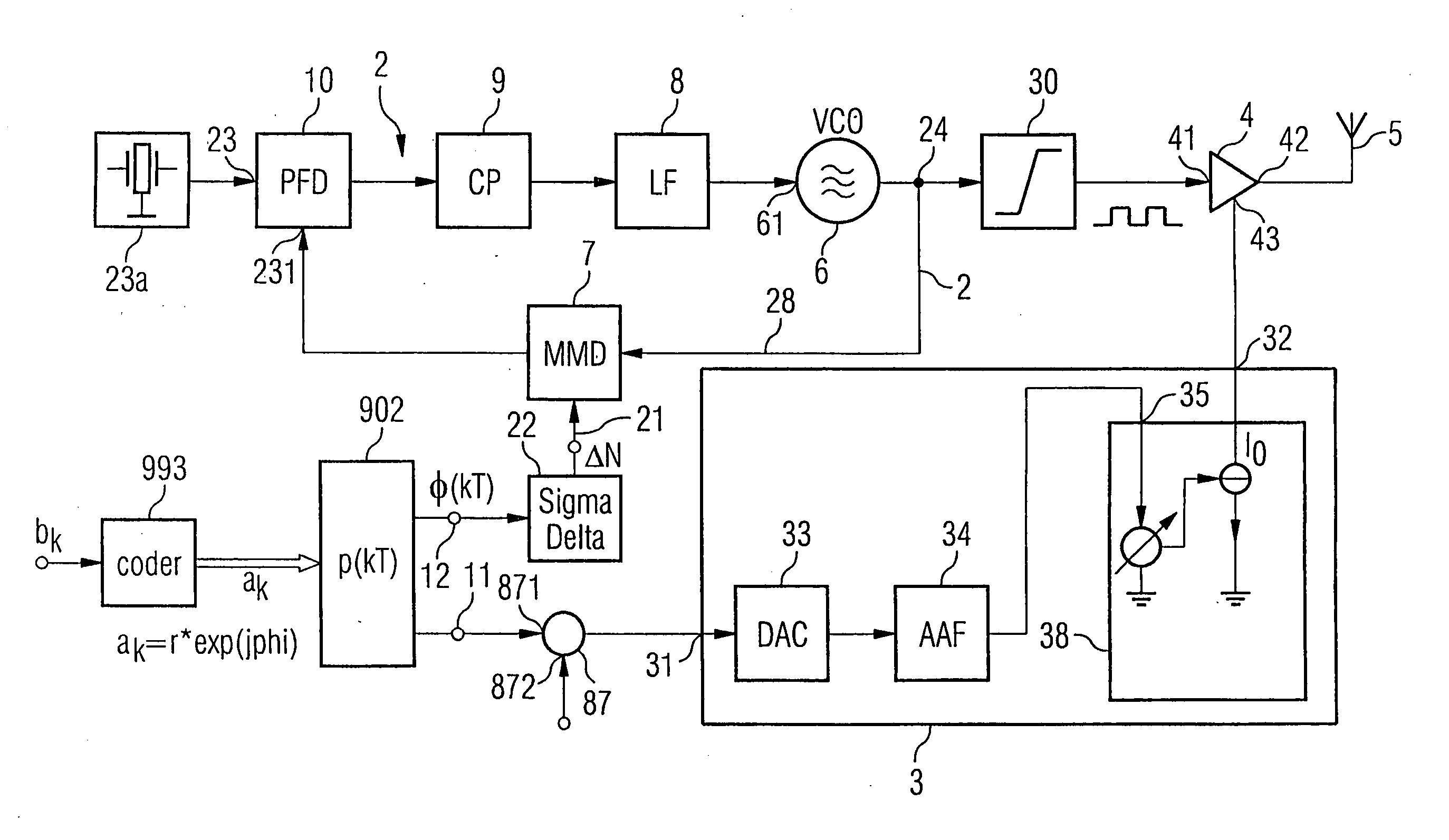
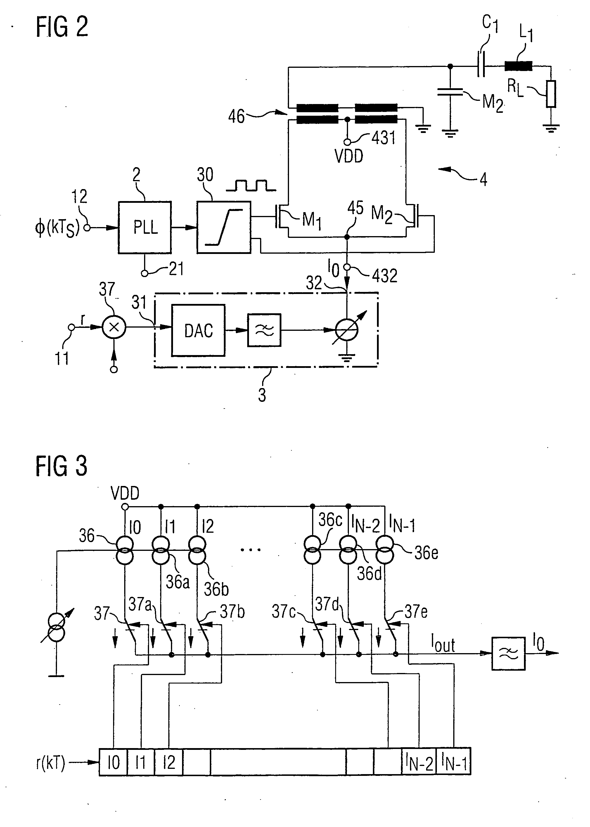
[0031] Turning to FIG. 1, a polar modulator according to one or more aspects of embodiments of the present invention is illustrated where the modulator is formed in a semiconductor body using CMOS technology. By way of example, silicon, g...


PUM


Abstract

A modulated carrier signal is produced from a phase modulation signal in a phase locked loop in a polar modulator. This carrier signal is converted via a limiting amplifier to a square-wave signal, which is supplied to an amplifier. At the same time, an amplitude modulation signal at one input is connected to a control input of a controllable current source. The controllable current source is designed to emit a supply current at a current output as a function of the amplitude modulation signal at the control input. The current output of the controllable current source is connected to a supply input of the amplifier. The supply current for the amplifier is thus modulated on the basis of the amplitude information to be transmitted. The processing of the amplitude information within the current domain makes it possible to produce the polar modulator according to the invention as an integrated circuit, using CMOS technology.

Description

REFERENCE TO RELATED APPLICATIONS [0001] This application claims the benefit of the priority date of German application DE 10 2004 060 177.1, filed on Dec. 14, 2004, the contents of which are herein incorporated by reference in their entirety. FIELD OF THE INVENTION [0002] One or more aspects or embodiments of the present invention relate to a polar modulator, and to a method for modulation of a signal. BACKGROUND OF THE INVENTION [0003] In modern communications systems, the information to be transmitted can be coded in phase and amplitude of a signal. This allows considerably greater data transmission rates to be achieved than with a pure amplitude modulation or phase modulation. Examples of modulation types such as these are PSK modulation (phase shift keying). These include, inter alia, π / 4 DQPSK, 8-DPSK or 8-PSK modulation. Quadrature amplitude modulation (QAM) also codes both the amplitude and the phase of the information to be transmitted. In contrast to analog amplitude or fr...

Claims


Application Information

Patent Timeline
Patent Type & Authority Applications(United States)
IPC IPC(8): H04B1/04H01Q11/12
CPCH03F3/24H03F2200/331H04L27/361
Inventor PUMA, GIUSEPPE LI
Owner INFINEON TECH AG
Why Eureka
Try Eureka