

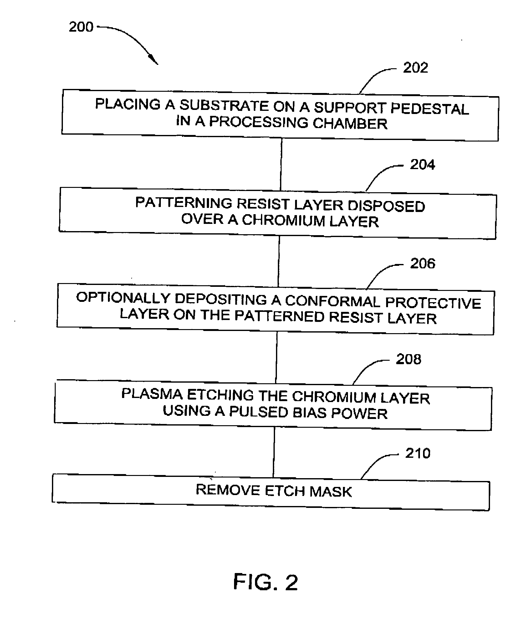
Method for plasma etching a chromium layer suitable for photomask fabrication
a chromium layer and plasma etching technology, applied in the field of plasma etching chromium, can solve the problems of affecting performance, unable to use masks, and conventional chromium etch processes often exhibit etch bias,
- Summary
- Abstract
- Description
- Claims
- Application Information
AI Technical Summary
Benefits of technology
Problems solved by technology
Method used
Image

Examples
Embodiment Construction
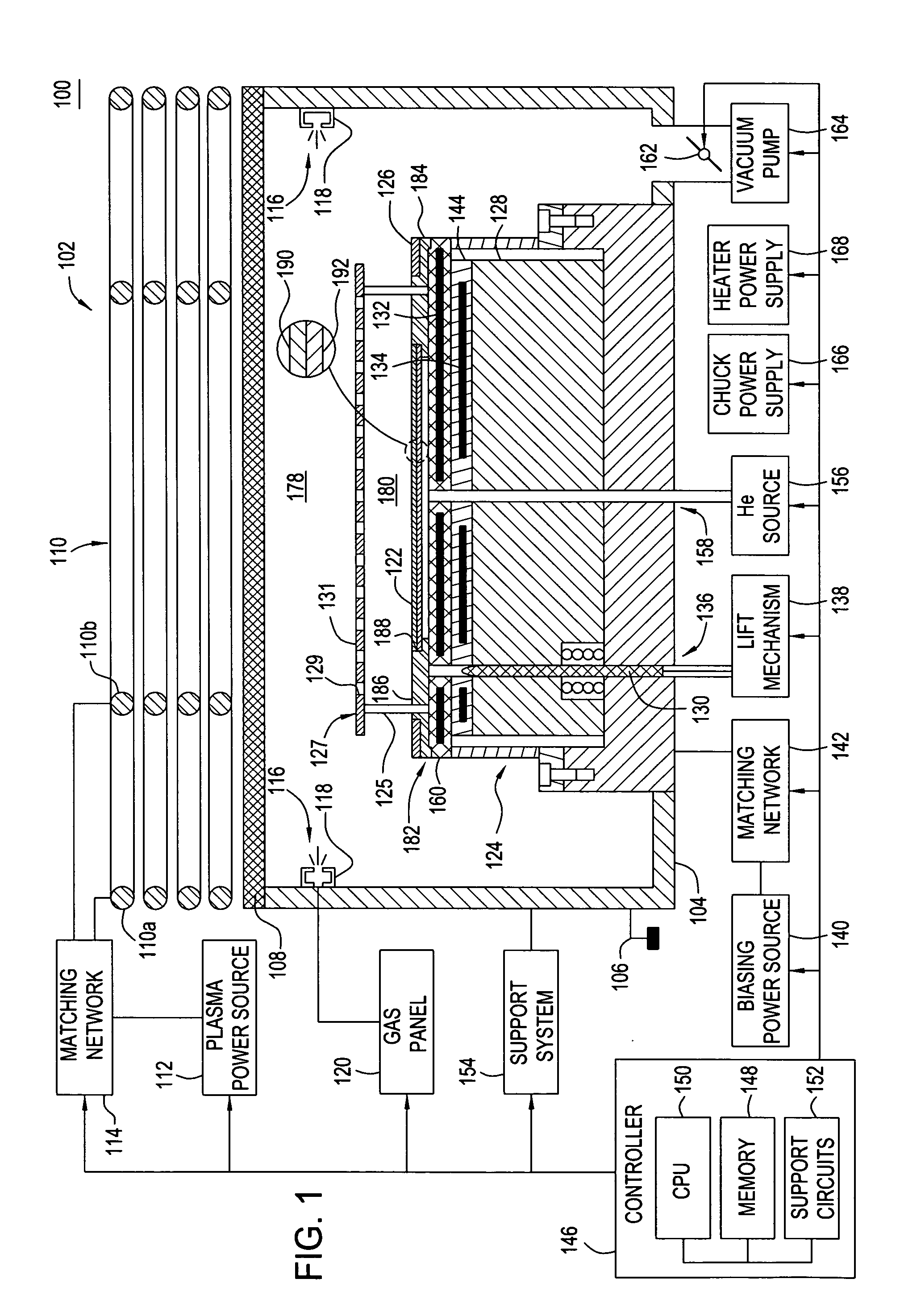
[0021]FIG. 1 depicts a schematic diagram of one embodiment of an etch processing chamber 100 in which a method of quartz etching of the present invention may be practiced. Suitable reactors that may be adapted for use with the teachings disclosed herein include, for example, the Decoupled Plasma Source (DPS®) II reactor, or the Tetra I and Tetra II Photomask etch systems, all of which are available from Applied Materials, Inc. of Santa Clara, Calif. The etch processing chamber 100 may also be used as a processing module of a processing system 170 as shown in FIG. 6, such as, for example, a Centura® integrated semiconductor wafer processing system, also available from Applied Materials, Inc. The processing system may also include a first chamber 172 suitable for ashing and a second chamber suitable for polymer deposition 174. Examples of suitable ashing and deposition chambers include AXIOM HT™ and Tetra II processing chamber, also available from Applied Materials, Inc. The particula...
PUM
| Property | Measurement | Unit |
|---|---|---|
| power | aaaaa | aaaaa |
| frequency | aaaaa | aaaaa |
| plasma power | aaaaa | aaaaa |
Abstract
Description
Claims
Application Information