Tunable active inductor

a technology of active inductor and resistor, which is applied in the direction of one-port active network, network simulating reactance, electrical apparatus, etc., can solve the problems of low resistance of cmos, difficult to implement a high-quality spiral inductor, and loss of microwave signals from silicon substrates with great loss of microwave signals, etc., to achieve the effect of resistor resistance value being tunabl

Active Publication Date: 2006-08-03
SAMSUNG ELECTRONICS CO LTD +1
View PDF9 Cites 19 Cited by
  • Summary
  • Abstract
  • Description
  • Claims
  • Application Information

AI Technical Summary

Problems solved by technology

However, when standard COMS technology is used for an RF part, the CMOS suffers a loss of microwave signals from silicon substrates with low resistance.
It has proven to be extremely difficult to implement a high-quality spiral inductor with silicon substrates having great microwave signal loss.
However, this approach is limited to only certain circuit structures.
However, the active inductor has the disadvantages of limited operation frequency range, high-noise characteristic, DC power consumption, and the like.
The active inductor of FIG. 1 has an advantage in that it provides a high gain and a high Q factor with a small size, but has a disadvantage of a very narrow operating frequency range between a zero frequency at and a gain bandwidth fT of the transistor M2.
Disadvantageously, however, the active inductor of FIG. 2 has a low gain and a low Q factor.
Basically, however, the active inductor of FIG. 3 has a disadvantage in that it is impossible to tune an inductance value, a self-resonant frequency ω, and a peak Q frequency fQ.
Furthermore, an increase in value of the feedback resistor Rf increases the inductance value but decreases the self-resonant frequency ω and the peak Q frequency fQ, making it difficult to use a high inductance value at a high frequency.

Method used


Image

  • Tunable active inductor
  • Tunable active inductor
  • Tunable active inductor

Examples


Embodiment Construction

[0032] A preferred embodiment of the present invention will now be described in detail with reference to the annexed drawings. In the following description, a detailed description of known functions and configurations incorporated herein has been omitted for conciseness.

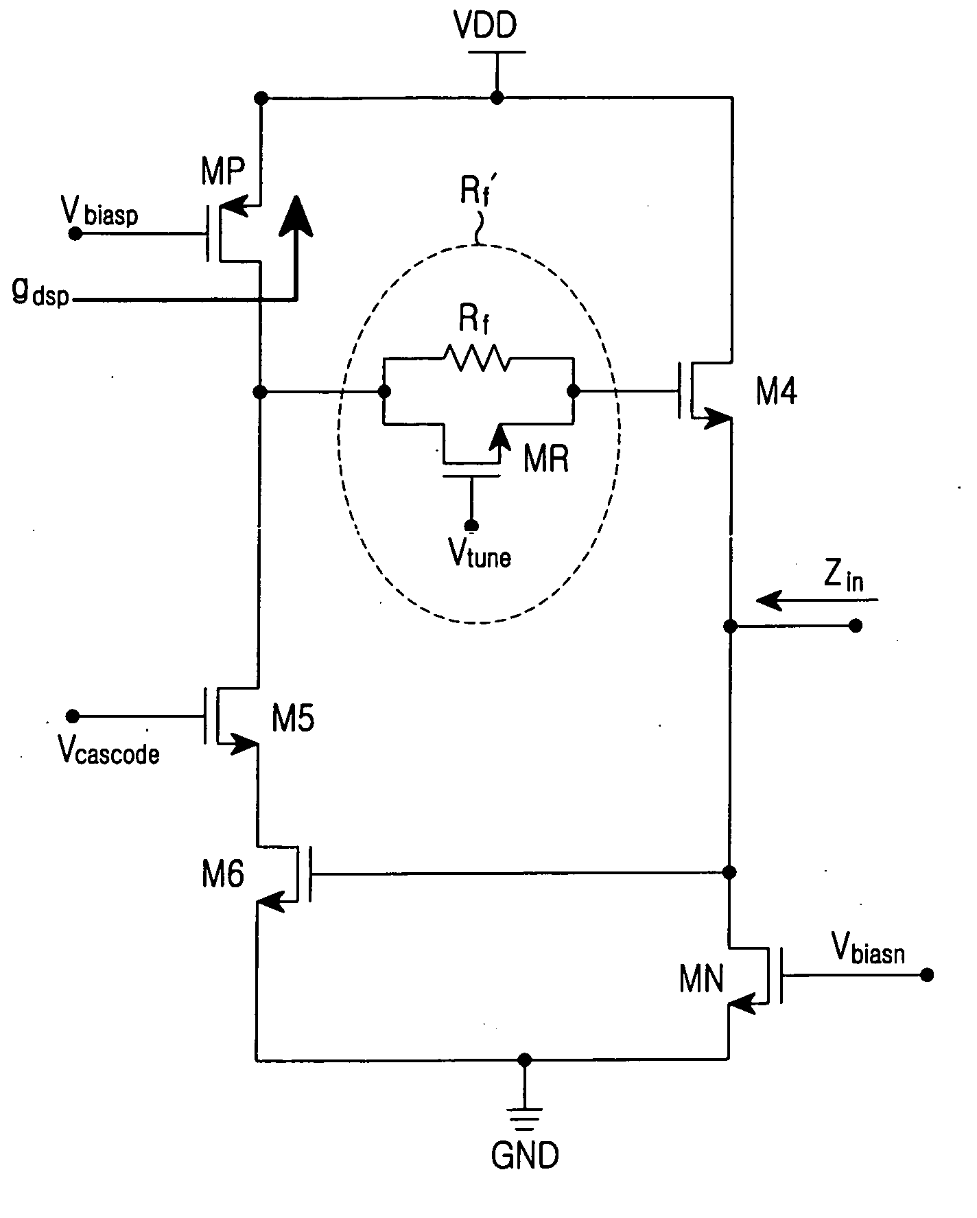
[0033]FIG. 4 is a circuit diagram of an active inductor according to an embodiment of the present invention. As illustrated in FIG. 4, an active inductor according to an embodiment of the present invention has the cascode-grounded structure with a tunable feedback resistor.

[0034] More specifically, the active inductor according to the present invention has a gyrator structure including a transistor M4 and a transistor M6, wherein a transistor M5 is connected to the transistor M6 in a cascode manner, and has a tunable feedback resistor Rf′ intervening between a drain of the transistor M5 and a gate of the transistor M4. A transistor MP, which is a PMOS-type transistor, serves as a current source, and a transistor MN...


PUM


Abstract

An active inductor capable of tuning a self-resonant frequency, an inductance, a Q factor, and a peak Q frequency by applying a tunable feedback resistor to a cascode-grounded active inductor is disclosed. The tunable active inductor includes a first transistor having a source connected to a power supply voltage and a gate connected to first bias voltage; a second transistor having a drain connected to a drain of the first transistor and a gate connected to a second bias voltage; a third transistor having a drain connected to a source of the second transistor and a source connected to a ground voltage; a fourth transistor having a drain connected to a gate of the third transistor, a source connected to the ground voltage and a gate connected to a third bias voltage; a fifth transistor having a source connected to the drain of the fourth transistor and a drain connected to the power supply voltage.

Description

PRIORITY [0001] This application claims the benefit under 35 U.S.C. §119 to a U.S. Provisional Patent Application entitled “TUNABLE ACTIVE INDUCTOR WITH VARIABLE RESISTIVE FEEDBACK AND ITS APPLICATION TO BROADBAND VOC's, filed in the United States Patent and Trademark Office on Feb. 2, 2005, and assigned Ser. No. 60 / 649,221, that contents of which are incorporated herein by reference.BACKGROUND OF THE INVENTION [0002] 1. Field of the Invention [0003] The present invention relates generally to a tunable active inductor, and in particular, to an active inductor with a high quality factor (Q factor) and a wide operating range, available for various radio frequency (RF) devices. [0004] 2. Description of the Related Art [0005] With the recent increasing demand for wireless personal communication systems, low-price and integrated processing technologies are required to reduce production cost and system size. [0006] The most preferable technology for wireless communication systems operatin...

Claims


Application Information

Patent Timeline
Patent Type & Authority Applications(United States)
IPC IPC(8): H03H11/00
CPCH03H11/50H03H11/48
Inventor MUKHOPADHY, RAJARSHINUTTINCK, SEBASTIENWOO, SANG-HYUNKIM, JONG-HANLEE, SEONG-SOOLEE, CHANG-HOLASKAR, JOY
Owner SAMSUNG ELECTRONICS CO LTD
Why Eureka
Try Eureka