Optical module

a technology of optical modules and optical components, applied in the field of optical modules, can solve the problems of increasing the value of the matching resistance, the power consumption of the device, and the mismatch of the impedance, so as to reduce the matching resistance, prevent the degradation of the signal reflection characteristic, and reduce the power loss

Active Publication Date: 2006-08-10
MITSUBISHI ELECTRIC CORP
View PDF11 Cites 28 Cited by
  • Summary
  • Abstract
  • Description
  • Claims
  • Application Information

AI Technical Summary

Benefits of technology

[0015] According to the present invention, the submount on which the LD device is mounted has a matching resistance and an interdigital capacitor formed thereon. The value of this matching resistance is set smaller than the impedance value of the signal source minus the resistance value of the LD d

Problems solved by technology

However, reducing the matching resistance leads to an impedance mismatch.
Conventional optical modules including a matching resistance have a problem in that the value of the matching resistance must be increased as the reference impedance to be matched increases.
Therefore, an increase in the matching resistance results in an increase in the power consumption of the device, because the LD device is current driven device.
This increases the parts count and hence cost, and makes it difficult to reduce the size of th

Method used


Image

  • Optical module
  • Optical module
  • Optical module

Examples


first embodiment

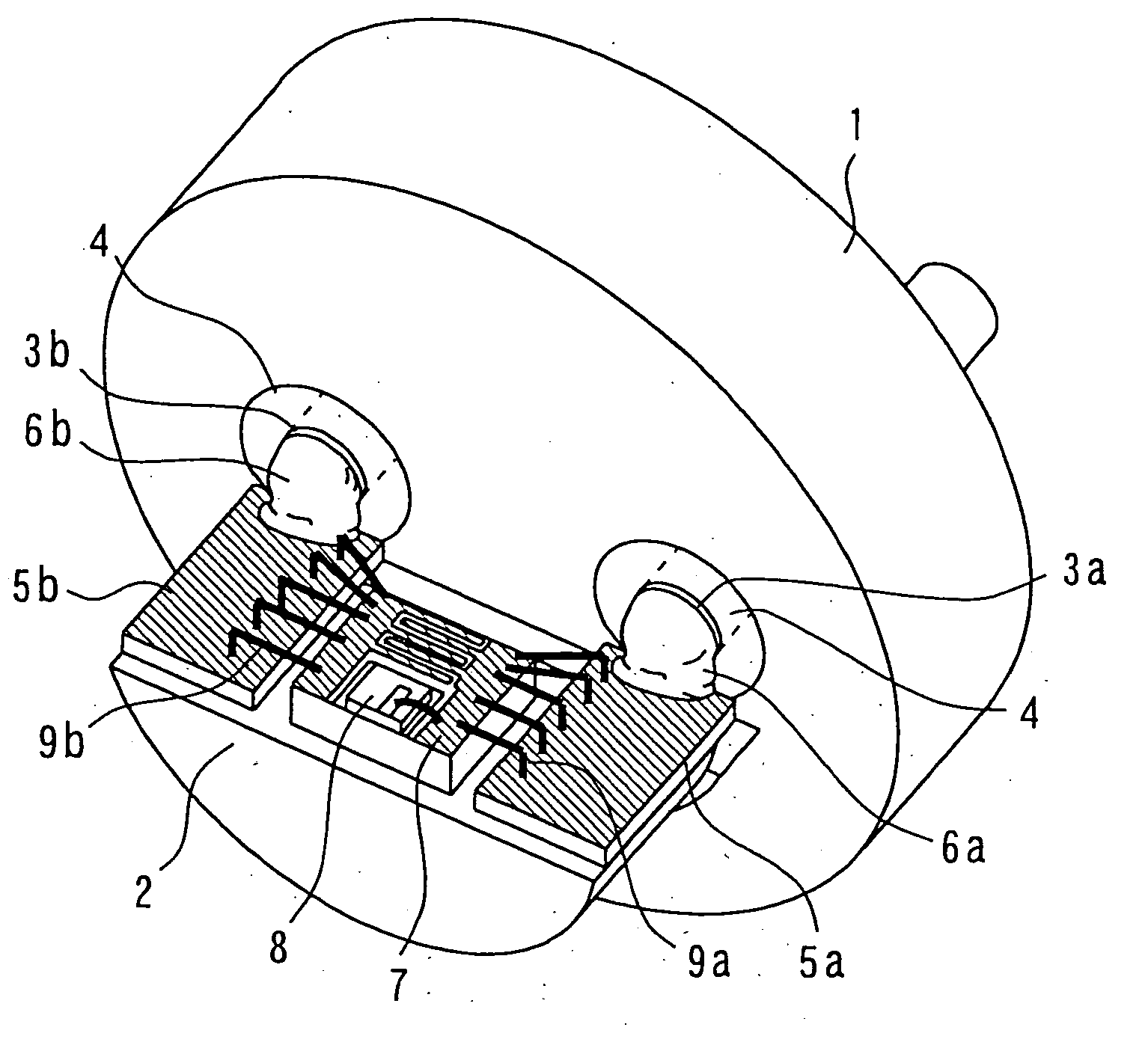
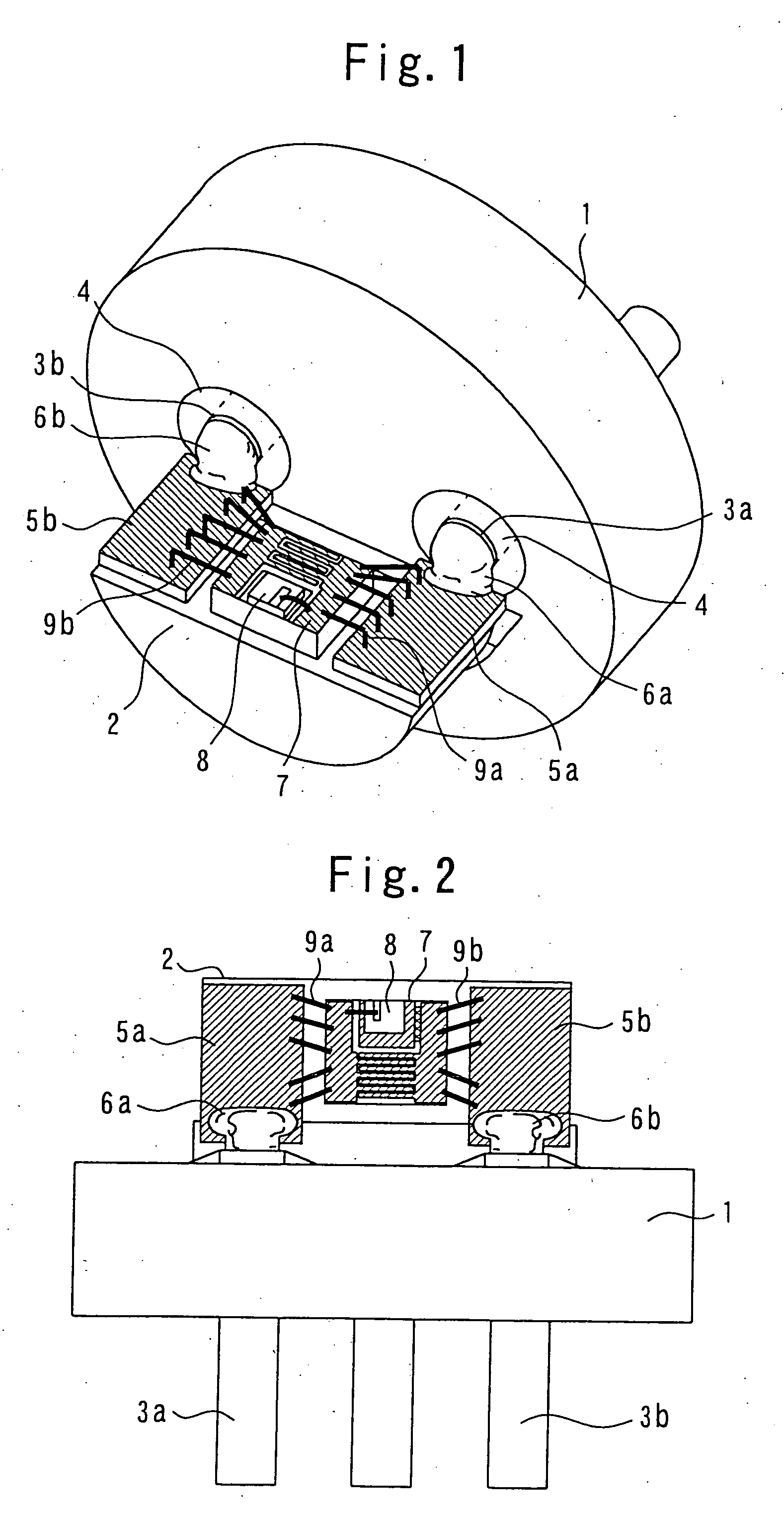
[0023]FIG. 1 is a perspective view of an optical module according to a first embodiment of the present invention; and FIG. 2 is a plan view of the optical module shown in FIG. 1.

[0024] Referring to FIGS. 1 and 2, a stem 1 has a mount block 2 fixed thereto and also has two lead pins 3a and 3b therethrough that enable for electrical connection to an external device and that transmit a differential signal to the optical module. Sealing glass 4 is filled between the lead pins 3a and 3b, and the through-holes of the stem 1, to fix the lead pins 3a and 3b to the stem 1 while electrically insulating them from each other and to seal between the inside and outside of the optical module. It should be noted that the cap (not shown) sealingly enclosing the mount block 2, etc. defines the exterior surface of the optical module.

[0025] Further, a submount 7 and interconnection substrates 5a and 5b are mounted on the mount block 2. The interconnection substrates 5a and 5b are disposed at position...

second embodiment

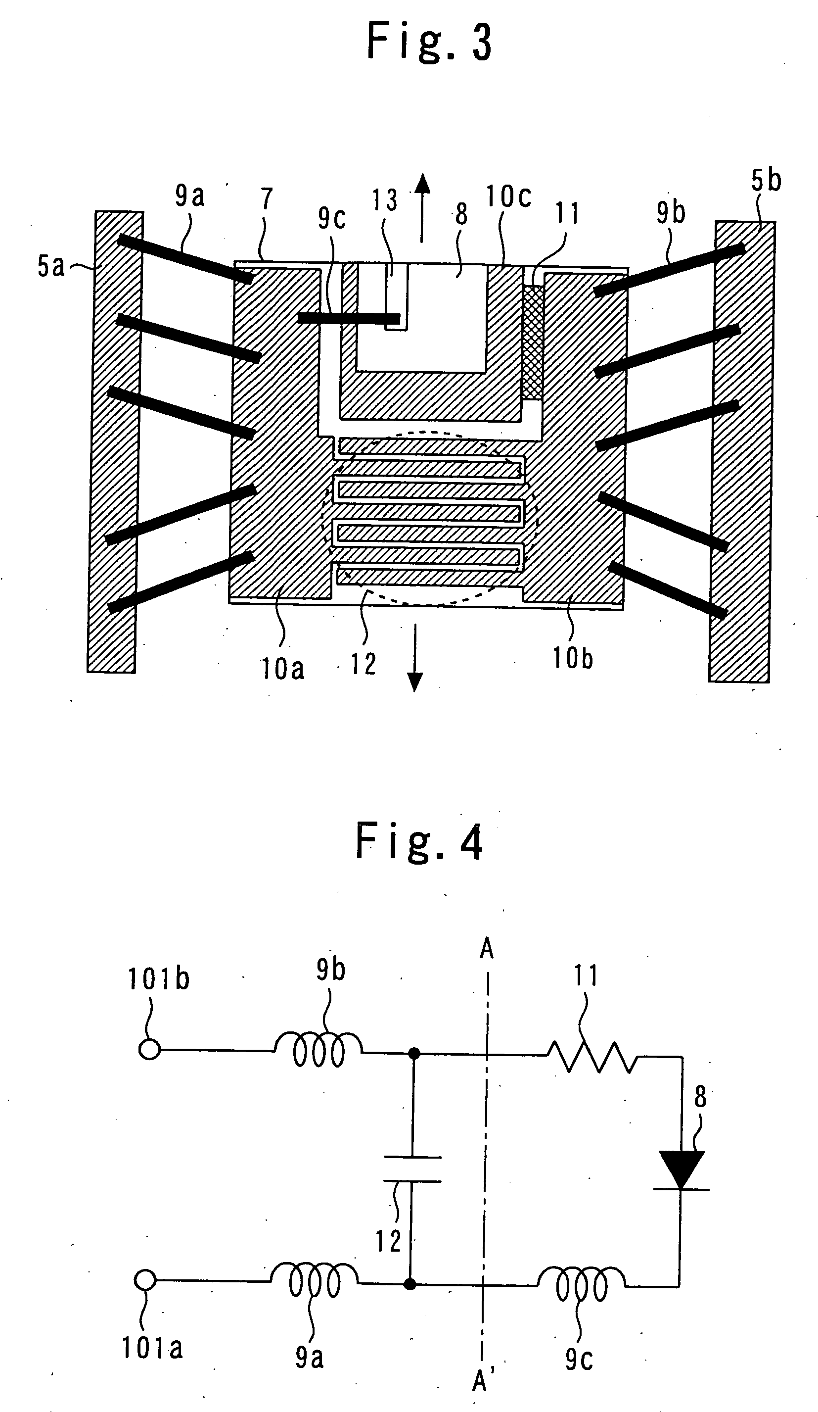
[0047]FIG. 7 is a perspective view of an optical module according to a second embodiment of the present invention. According to the first embodiment, the submount 7 is electrically connected to the lead pins 3a and 3b through the interconnection substrates 5a and 5b, respectively, whose impedance is suitably adjusted, as described above. (The interconnection substrates 5a and 5b are disposed so as to sandwich the submount 7.) Therefore, the interconnection electrode patterns 10a and 10b of the submount 7 are connected to the interconnection substrates 5a and 5b by the wire bonds 9a and 9b, respectively. On the other hand, the optical module of the second embodiment is configured such that: the lead pins 3a and 3b (renamed as lead pins 3A and 3B) are extended so as to sandwich the submount 7; and these lead pins 3A and 3B are directly connected to the interconnection electrode patterns 10a and 10b by the wire bonds 9a and 9b, respectively. It should be noted that all other components...


PUM


Abstract

An optical module includes a stem; a first lead pin and a second lead pin for receiving differential signals, the first and second lead pins penetrating the stem; a mount block fixed to the stem; a laser diode having a pair of electrodes; a submount mounted on the mount block and having a matching resistance, an interdigital capacitor, and a plurality of electrode patterns on a surface on the submount; and a first wire and a second wire electrically connecting the submount to the first and second lead pins, respectively. The laser diode is mounted on one of the electrode patterns on the submount and connected to another one of the electrode patterns on the submount by a third wire such that the laser diode, together with the matching resistance and the interdigital capacitor, forms an electrical circuit. The value of the matching resistance is smaller than an impedance value of a differential signal source supplying the differential signals minus the resistance of the laser diode.

Description

BACKGROUND OF THE INVENTION [0001] 1. Field of the Invention [0002] The present invention relates to an optical module employing a laser diode device, and more particularly to an optical module used for high speed optical communications, which require impedance matching. [0003] 2. Background Art [0004] In recent years, there has been a need to reduce the power consumption and the size of optical modules for communications employing a laser diode device (or LD device), as well as to increase the speed of the modulating signal (more than 10 GHz). [0005] Because the faster speed of the modulating signal handled by an optical module includes the more high frequency components in the modulating signal, the transmission lines etc. within the optical module must be impedance matching well for high frequency signals. [0006] Therefore, conventional optical modules are configured such that: a matching resistance is provided between the LD device and the driver circuit for driving the LD devic...

Claims


Application Information

Patent Timeline
IPC IPC(8): H01S3/00
CPCH01S5/02212H01S5/02248H01S5/02276H01S5/0427H01S5/06226H01L2224/48091H01L2224/48227H01L2924/19107H01S5/02325H01S5/02345H01L2924/00014
Inventor ARUGA, HIROSHI
Owner MITSUBISHI ELECTRIC CORP
Why Eureka
Try Eureka