Laser diode packaging

a technology of laser diodes and packaging, applied in the field of packaging, can solve the problems of reducing the utilization rate of laser diodes, reducing the efficiency of laser diodes, and increasing the difficulty of dissipation of heat, so as to achieve the effect of minimizing thermal resistance and small dimensions

Inactive Publication Date: 2006-08-24
NORTHROP GRUMMAN SYST CORP +1
View PDF67 Cites 11 Cited by
  • Summary
  • Abstract
  • Description
  • Claims
  • Application Information

AI Technical Summary

Benefits of technology

[0013] A laser diode package and a laser diode array that are constructed in this manner lack the hazardous beryllium oxide. More importantly, each individual package has its own electrical isolation and can be directly soldered to an ultimate heat sink. Furthermore, each individual package can be tested on its own before being placed in an array to ensure that it will function within the operational parameters (e.g. wavelength and power) desired for such an array. When the substrate is made of a cleaveable material such as GaAs, it can be produced with relatively small dimensions thereby minimizing the thermal resistance between the laser diode and the ultimate heat sink. The resulting laser diode package can be used for continuous wave (CW) modes of operation or for pulsed modes of operation.

Problems solved by technology

Universal utilization of semiconductor laser diodes has been restricted by thermally related problems.
These problems are associated with the large heat dissipation per unit area of the laser diodes which results in elevated junction temperatures and stresses induced by thermal cycling.
When solid state laser rods or slabs are pumped by laser diodes, dissipation of the heat becomes more problematic since it becomes necessary to densely pack a plurality of individual diodes into arrays which generate the required amounts of input power for the larger, solid state laser rod or slab.
However, when the packing density of the individual laser diodes is increased, the space available for extraction of heat from the individual laser diodes decreases.
This aggravates the problem of heat extraction from the arrays of individual diodes.
However, beryllium oxide is a hazardous material and requires additional care in handling.
Because it requires additional care in handling and shipping (e.g. additional BeO warning labels), it is relatively expensive when considering the cost of the overall laser diode array package.
Additionally, once the laser diode bar is placed within the groove, its reflective surface is not accessible for cleaning after the array has been assembled.
Furthermore, it is difficult to test an individual laser diode bar before it is placed in the grooves.
Thus, a laser diode bar lacking the desired operational characteristics for a specific array must often be removed from a groove after it has been installed.

Method used


Image

  • Laser diode packaging
  • Laser diode packaging
  • Laser diode packaging

Examples


Embodiment Construction

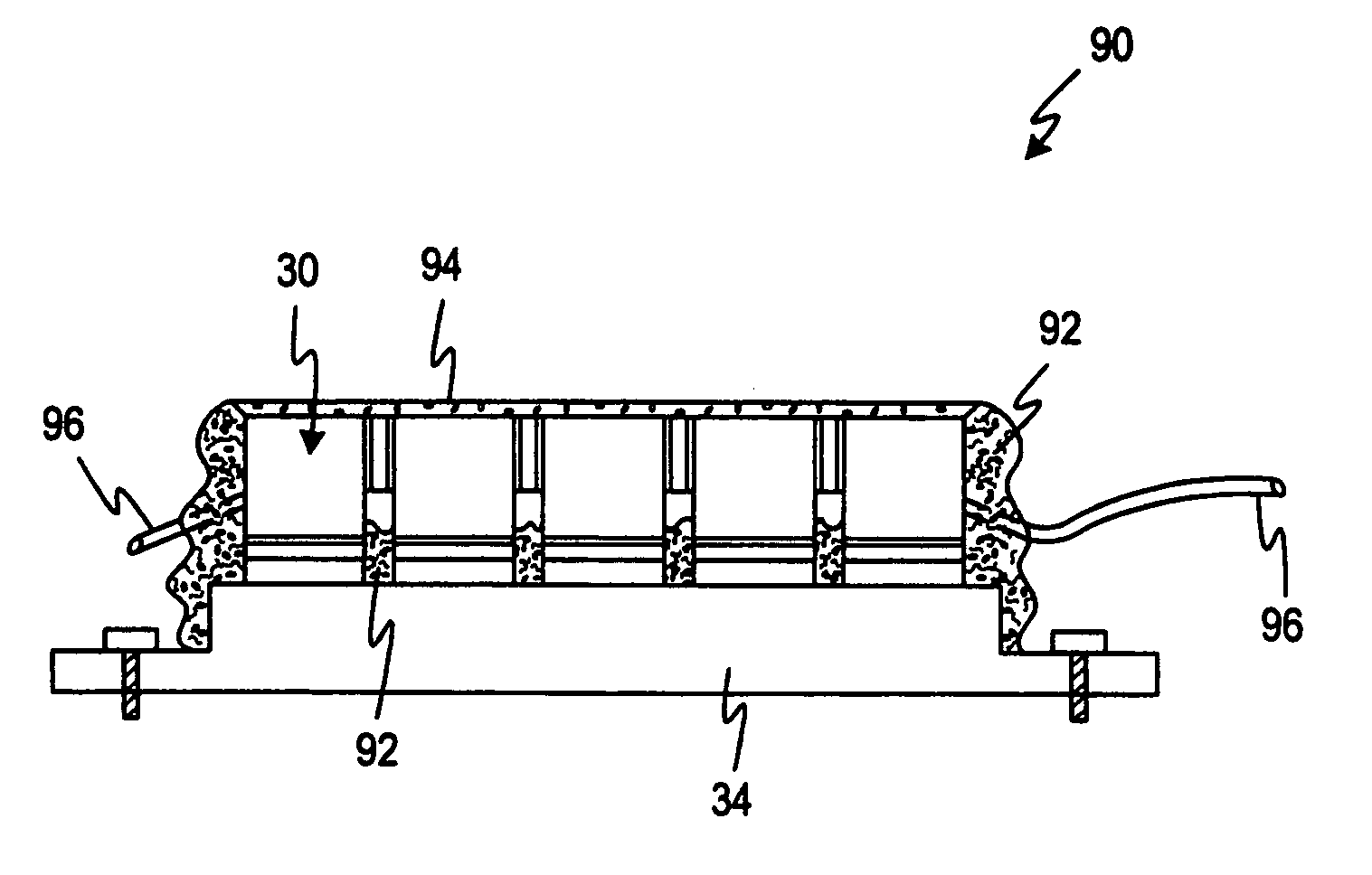
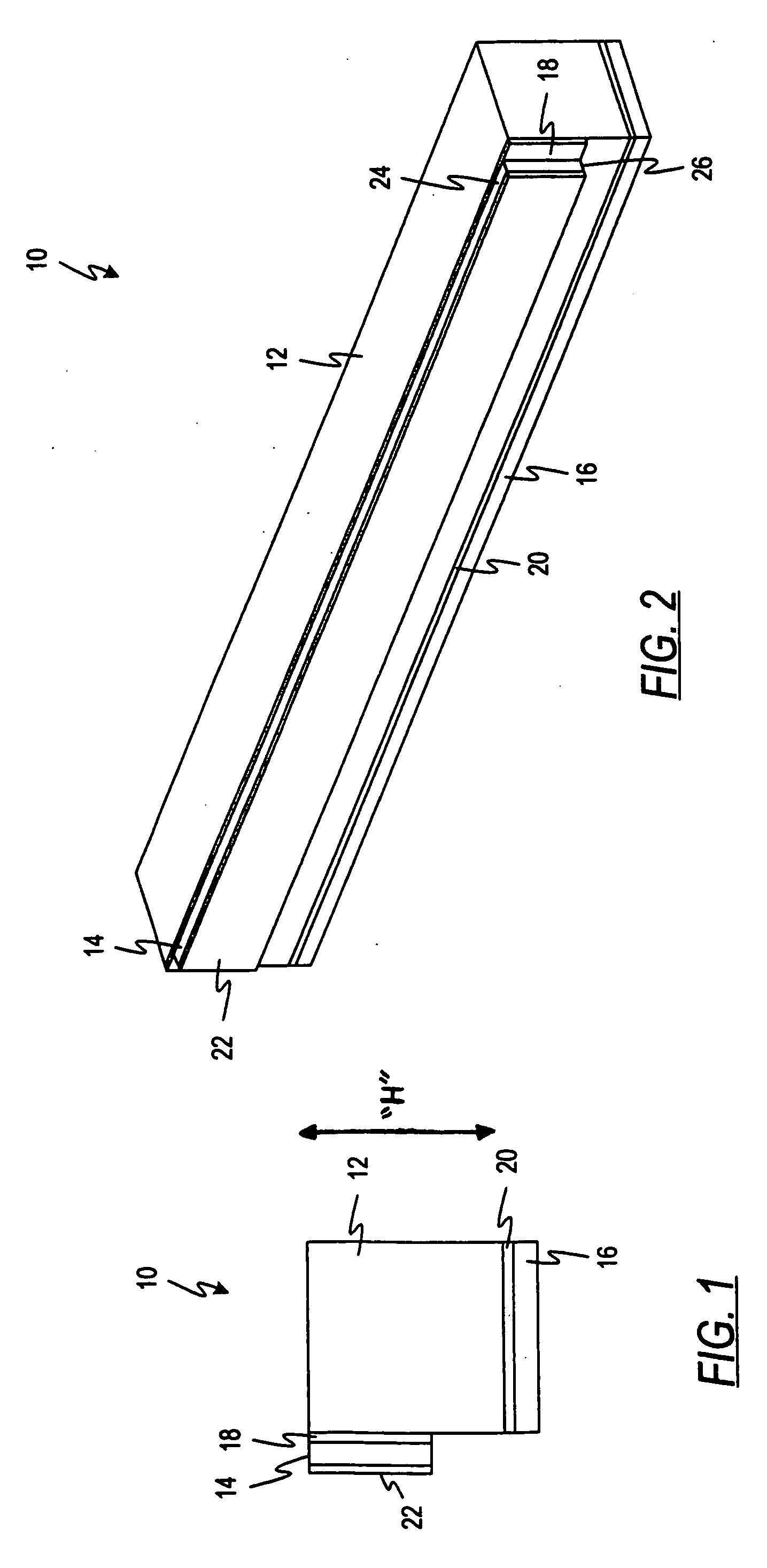
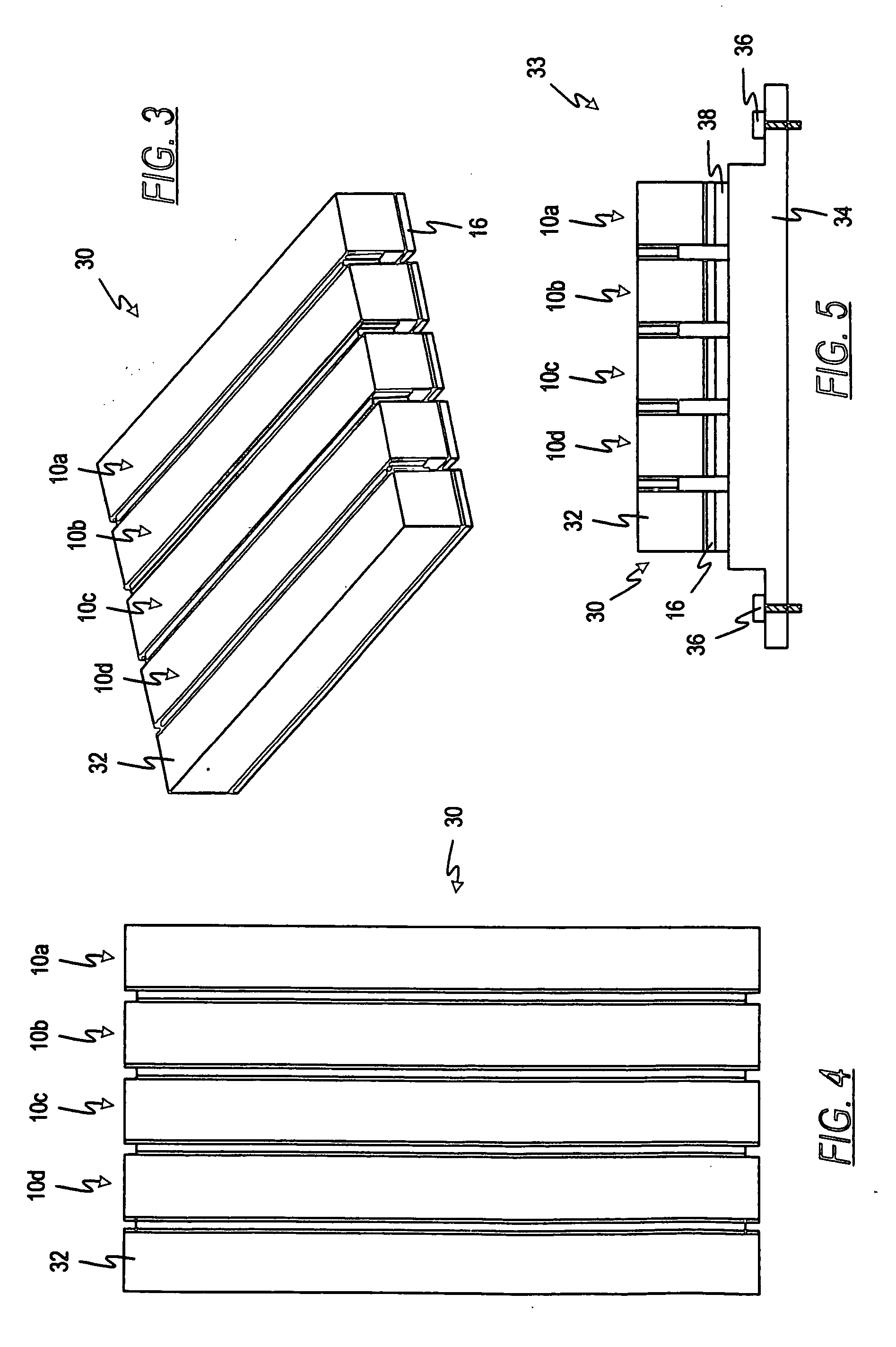
[0033] Referring initially to FIGS. 1 and 2, a laser diode package 10 includes a heat sink 12, a laser diode bar 14, and a lower substrate 16. The laser diode bar 14 is attached to the heat sink 12 through a first solder layer 18. The substrate 16 is attached to the heat sink 12 through a second solder layer 20. The laser diode bar 14 may also include a bar solder layer 22 on its side which opposes the heat sink 12. The method by which such a bar solder layer 22 is applied is described in detail with respect to FIGS. 8-11.

[0034] The laser diode bar 14 has an emitting surface 24 at its upper end and a reflective surface 26 that opposes the emitting surface 24. The height of the laser diode bar 14 is defined as the distance between the emitting surface 24 and reflective surface 26. The junction of the laser diode 14, which is the region at which the photons are emitted from the laser diode bar 14, is typically closer to the heat sink 12. However, the junction of the laser diode bar 1...


PUM


Abstract

A laser diode package includes a heat sink, a laser diode, and an electrically nonconductive (i.e. insulative) substrate. The laser diode has an emitting surface and a reflective surface opposing the emitting surface. The laser diode further has first and second side surfaces between the emitting and reflective surfaces. The heat sink has an upper surface and a lower surface. The first side surface of the laser diode is attached to the heat sink adjacent to the upper surface. The substrate is attached to the lower surface of the heat sink. The heat sink is made of heat conducting metal such as copper and the substrate is preferably made from gallium arsenide. The substrate is soldered to the heat sink as is the laser diode bar. Due to the presence of the substrate at the lower end of the heat sink, each individual laser diode package has its own electrical isolation. Several packages can be easily attached together to form a laser diode array.

Description

FIELD OF THE INVENTION [0001] The present invention relates generally to lasers diodes and, in particular, to a package for a laser diode that is easy to manufacture, has a low thermal resistance, and requires no beryllium oxide. BACKGROUND OF THE INVENTION [0002] Semiconductor laser diodes have numerous advantages. They are small in that the widths of their active regions are typically submicron to a few microns and their heights are usually no more than a fraction of a millimeter. The length of their active regions is typically less than about a millimeter. The internal reflective surfaces, which produce emission in one direction, are formed by cleaving the substrate from which the laser diodes are produced and, thus, have high mechanical stability. [0003] High efficiencies are possible with semiconductor laser diodes with some pulsed junction laser diodes having external quantum efficiencies near 50%. Semiconductor lasers produce radiation at wavelengths from about 20 to about 0....

Claims


Application Information

Patent Timeline
Patent Type & Authority Applications(United States)
IPC IPC(8): H01L31/0203H01L23/34H01S5/022H01S5/02H01S5/024H01S5/40
CPCH01S5/005H01S5/02248H01S5/02264H01S5/02272H01S5/02423H01S5/4018H01S5/405H01S5/02325H01S5/02365H01S5/0237
Inventor STEPHENS, EDWARD F.
Owner NORTHROP GRUMMAN SYST CORP
Why Eureka
Try Eureka