Electron emitting element and image forming apparatus employing it

a technology of electron emitting element and image forming apparatus, which is applied in the direction of instruments, tubes with screens, corona discharge, etc., can solve the problems of sputtering and breakdown of elements, and achieve the effect of stable operation

Active Publication Date: 2006-08-24
KOSHIDA NOBUYOSHI +1
View PDF1 Cites 39 Cited by
  • Summary
  • Abstract
  • Description
  • Claims
  • Application Information

AI Technical Summary

Problems solved by technology

This has resulted in a problem that plus ions generated by ionization of gas molecules are accelerated by the strong electric field in the direction toward the element surface and collide with the element surface, causing element breakdown due to sputtering.
In a case where such an element is operated in the atmosphere, however, a problem has newly occurred that various gas molecules are adsorbed on a surface of the element to change an electric characteristic or the like of the semiconductor and to thereby reduce an electron emission current.
Therefore, in a case where an electron emitting element is operated in the atmosphere, a problem arises that gas molecules intrude into an inside semiconductor layer to change an electric characteristic or the like of the semiconductor to thereby reduce an electron emission current.

Method used


Image

  • Electron emitting element and image forming apparatus employing it
  • Electron emitting element and image forming apparatus employing it
  • Electron emitting element and image forming apparatus employing it

Examples


embodiment 1

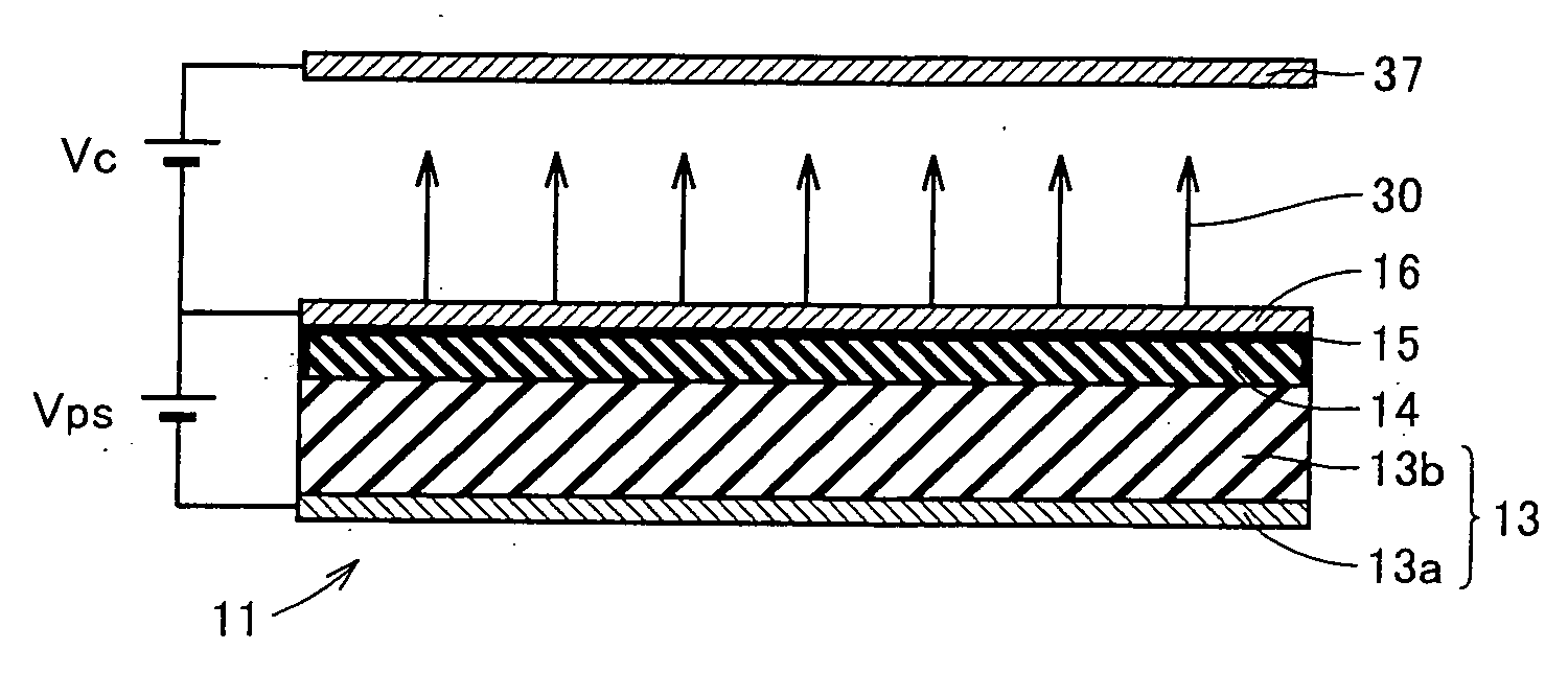
[0041] With reference to FIG. 1, an electron emitting element 11 according to the present invention has a structure in which a porous polysilicon layer as a semiconductor layer 14 is formed on a semiconductor substrate 13b made of n-type silicon on the rear surface of which an ohmic electrode 13a is formed, an organic compound is caused to be adsorbed on a polysilicon surface of the porous polysilicon layer to form an organic compound adsorption layer 15, and an upper electrode 16 is formed on a surface thereof. Not only is organic compound adsorption layer 15 shown in FIG. 1 formed on a surface of the porous polysilicon layer, but an organic compound adsorption layer is formed on a polysilicon surface in the inside of the porous polysilicon layer, though not shown. Semiconductor substrate 13b made of n-type silicon has a high electric conductivity and has a function as a lower electrode 13 integrally in a piece with ohmic electrode 13a.

[0042] The porous polysilicon layer was prepa...

embodiment 2

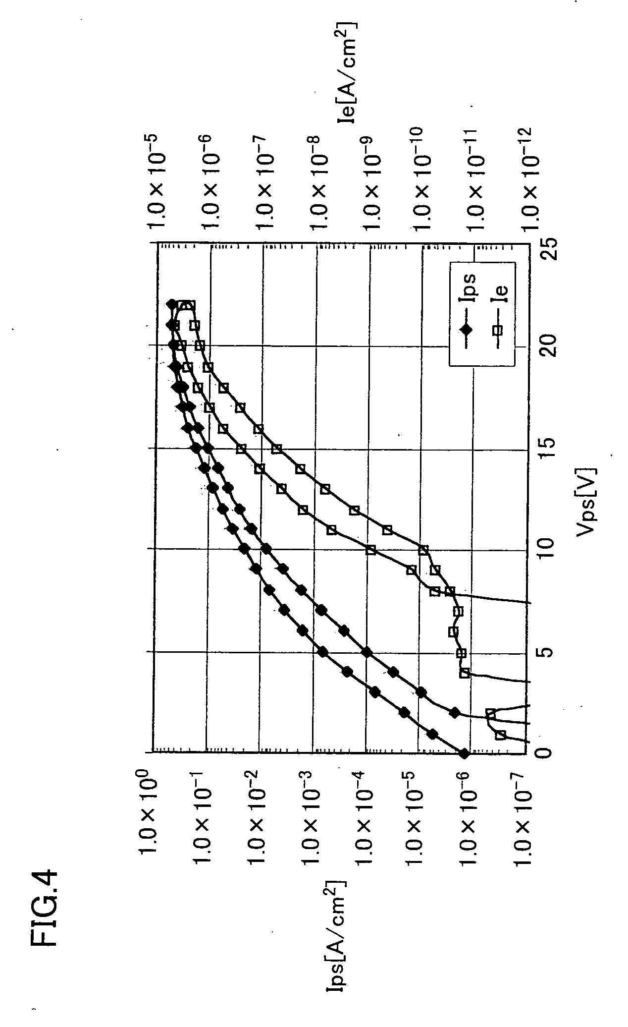
[0053] Another electron emitting element according to the present invention (an inventive element in the example shown in FIG. 7) was fabricated in a similar way to that in Embodiment 1 with the exception that n-dodecanal (CH3(CH2)10CHO) was used when an organic compound is adsorbed on a polysilicon surface of a porous polysilicon layer. FIG. 7 shows a change in electron emission current quantity with a heavy line while the inventive element was continuously driven in a similar way to that in Embodiment 1. A fine line in FIG. 7 shows a change in electron emission quantity of a conventional electron emitting element having a semiconductor surface of a semiconductor layer on which no organic compound is adsorbed (a conventional element in the comparative example of FIG. 7) with a fine line while the conventional element was operated continuously in the same way. As shown in FIG. 7, by causing n-dodecanal to be absorbed on a surface of a semiconductor layer, an electron emission curren...

embodiment 3

[0054] Electron emitting element 11 according to the present invention was obtained in a similar way to that in Embodiment 1 with the exception that 1-decene (CH3(CH2)7CH═CH2) was used when an organic compound was caused to be adsorbed on a silicon surface of a porous polysilicon layer. By adsorption of 1-decene to the silicon surface of a porous polysilicon layer, a reaction occurs, as shown in FIG. 9, between hydrogen terminals remaining on the porous polysilicon surface and a vinyl group of 1-decene and as a result, a long chain alkyl group (n=9) of 1-decene is chemically adsorbed on the polysilicon surface to thereby form an organic compound adsorption layer.

[0055] Note that an adsorption state of an organic compound, that is a state of an organic compound adsorption layer, on the silicon surface can be analyzed with DRIFT (Diffuse Reflectance Infrared Fourier-transform), Auger electron spectroscopy, Raman spectroscopy or the like.


PUM


Abstract

An electron emitting element is of a structure in which a semiconductor layer is formed between an upper electrode and a lower electrode, wherein an organic compound adsorption layer is formed on a semiconductor surface of the semiconductor layer by causing the organic compound to be adsorbed on the semiconductor surface. Herein, the semiconductor layer can be made of silicon or polysilicon and partly or as a whole porous. The absorbed organic compound can be a non-cyclic hydrocarbon, a compound obtained by coupling at least an aldehyde group to a non-cyclic hydrocarbon, or a non-cyclic hydrocarbon having an unsaturated bond. As a result, there can be provided an electron emitting element capable of stably operating in the atmosphere or in a low vacuum even when being operated in the atmosphere or in the low vacuum and an imaging device using the electron emitting element.

Description

TECHNICAL FIELD [0001] The present invention relates to an electron emitting element capable of stably operating for a long period of time even in the atmosphere, and an imaging device using the same. BACKGROUND ART [0002] A Spindt-type electrode, a carbon nanotube (CNT)-type electrode and the like have been known as conventional cold cathode-type electron emitting elements, which have been studied on applications to the field of FED (Field Emission Display). The elements are operated in such a manner that a voltage is applied to a pointed end to form a strong electric field of about 1 GV / m and to emit electrons with the help of a tunneling effect. [0003] There has been heretofore present an idea that such an electron emitting element is operated in the atmosphere and applied to a charger or an electrostatic latent image forming device. For example, there has been proposed a method in which a Spindt-type cold cathode is operated in the atmosphere to emit electrons into the atmospher...

Claims


Application Information

Patent Timeline
Patent Type & Authority Applications(United States)
IPC IPC(8): H01J63/04H01J1/62G03G15/02H01J1/312H01J31/12
CPCG03G15/0291
Inventor IWAMATSU, TADASHIHIRAKAWA, HIROYUKIKOSHIDA, NOBUYOSHI
Owner KOSHIDA NOBUYOSHI
Why Eureka
Try Eureka