Unlock instant, AI-driven research and patent intelligence for your innovation.

Serial audio output driver circuits and methods

a driver circuit and audio output technology, applied in logic circuit coupling/interface arrangement, pulse technique, instruments, etc., can solve the problems of serial output driver digital noise coupling onto the device substrate, inability to re-timing, and inability to meet device operating parameters, so as to minimize the transmission of noise generated on the substrate and minimize the effect of source-to-gate overvoltag

Active Publication Date: 2006-08-24
CIRRUS LOGIC INC
View PDF9 Cites 2 Cited by
  • Summary
  • Abstract
  • Description
  • Claims
  • Application Information

AI Technical Summary

Benefits of technology

[0008] Embodiments of the present principles advantageously utilize PMOS output voltage pull-up and pull-down transistors to minimize substrate transmission of noise generated during serial port output switching. These principles are especially advantageous in mixed-signal circuits, although the range of potential applications is much broader. Additionally, gate charge pumping circuitry is disclosed which ensures that the PMOS output pull-down transistors pull-down the output voltage substantially to zero volts. Furthermore, an additional PMOS output pull-down transistor is disclosed which initiates output voltage pull-down operations and thereby minimizes source-to-gate overvoltage across the primary PMOS output pull-down transistors.

Problems solved by technology

One frequent problem experienced with ADC serial output ports is the coupling of digital noise onto the device substrate from the serial output driver driving the SDOUT output, especially when the SDOUT output is driving a relatively high load.
However, in the slave mode, in which the SCLK signal is typically received with an arbitrary phase relationship with the external and / or internal MCLK signals, re-timing is often not possible.
In particular, for higher frequency SCLK signals, the timing window between the SCLK signal and the internal MCLK signal may be too small to meet device operating parameters, such as set-up time.

Method used


Image

  • Serial audio output driver circuits and methods
  • Serial audio output driver circuits and methods
  • Serial audio output driver circuits and methods

Examples


Embodiment Construction

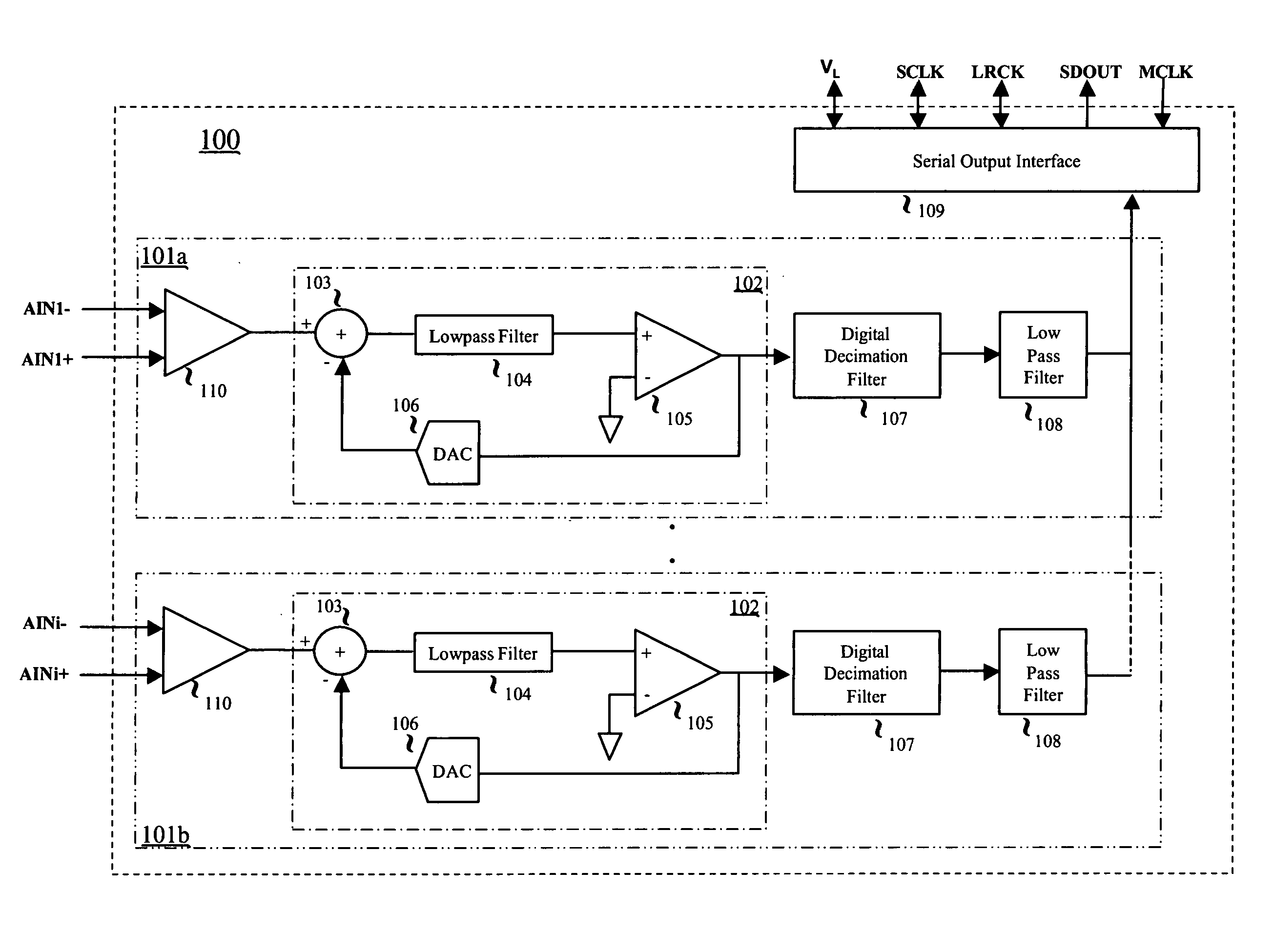
[0013] The principles of the present invention and their advantages are best understood by referring to the illustrated embodiment depicted in FIGS. 1-3 of the drawings, in which like numbers designate like parts.

[0014]FIG. 1 is a high level operational block diagram of a single-chip audio analog-to-digital converter (ADC) 100 suitable for describing the principles of the present invention. ADC 100 is only one of a number of possible applications in which the principles can advantageously be utilized. Other examples include general purpose ADCs, digital to analog converters (DACs), and encoder-decoders (Codecs).

[0015] ADC 100 includes n-number of conversion paths, of which 101a and 101b are shown for reference, for converting n-number of channels of analog audio data respectively received at left and right analog differential inputs AINn+ / −, where n is the channel number from 1 to n. The analog inputs for each channel in the illustrated embodiment are passed through an input gain ...


PUM


Abstract

An output driver circuit including a transistor for pulling down an output terminal voltage and a charge pump for driving an input of the transistor to pull-down the output terminal voltage substantially to zero volts in response to a selected level of an input signal.

Description

FIELD OF INVENTION [0001] The present invention relates in general to mixed signal techniques, and in particular, to serial audio output driver circuits and methods. BACKGROUND OF INVENTION [0002] Many audio applications, such as audio analog to digital converters (ADCs) and audio encoder—decoders (CODECs), utilize a serial data port to transmit digitized audio data to other devices in a system. A typical audio serial data port outputs bits of a serial audio data (SDOUT) stream in response to an associated serial clock (SCLK) signal. In a stereo system, two channels of audio data are time-multiplexed onto the SDOUT stream with a left-right clock (LRCK) signal. Overall timing is controlled by a master clock (MCLK) signal. Advantageously, the utilization of serial ports minimizes the number of pins and associated on-chip driver circuitry. [0003] A typical serial data port operates in either a master mode or a slave mode. In the master mode, the SCLK and LRCK clock signals are generate...

Claims


Application Information

Patent Timeline
Patent Type & Authority Applications(United States)
IPC IPC(8): H03M1/12
CPCH03F3/2175H03F2200/03H03F2200/331H03K19/00315H03K19/00361H03K19/018557H03M3/02
Inventor WELSER, JOSEPH JASONGABORIAU, JOHANN GUY
Owner CIRRUS LOGIC INC