Manufacture method for semiconductor device having field oxide film

Inactive Publication Date: 2006-08-24
YAMAHA CORP
View PDF2 Cites 5 Cited by
  • Summary
  • Abstract
  • Description
  • Claims
  • Application Information

AI Technical Summary

Benefits of technology

[0058] According to the second semiconductor device manufacture method, in the device forming region of the one conductivity type, the channel stopper region can be formed easily and at high precision just under the field oxide film and being spaced apart from the device opening. Since the number of processes is small, a manufacture yield can be improved and cost reduction can be achieved.
[0059] According to the third semicon

Problems solved by technology

However, with the existence of only the side wall, it is difficult to form the channel stopper ion doped region spaced apart from the device opening of the field o

Method used


Image

  • Manufacture method for semiconductor device having field oxide film
  • Manufacture method for semiconductor device having field oxide film
  • Manufacture method for semiconductor device having field oxide film

Examples


first embodiment

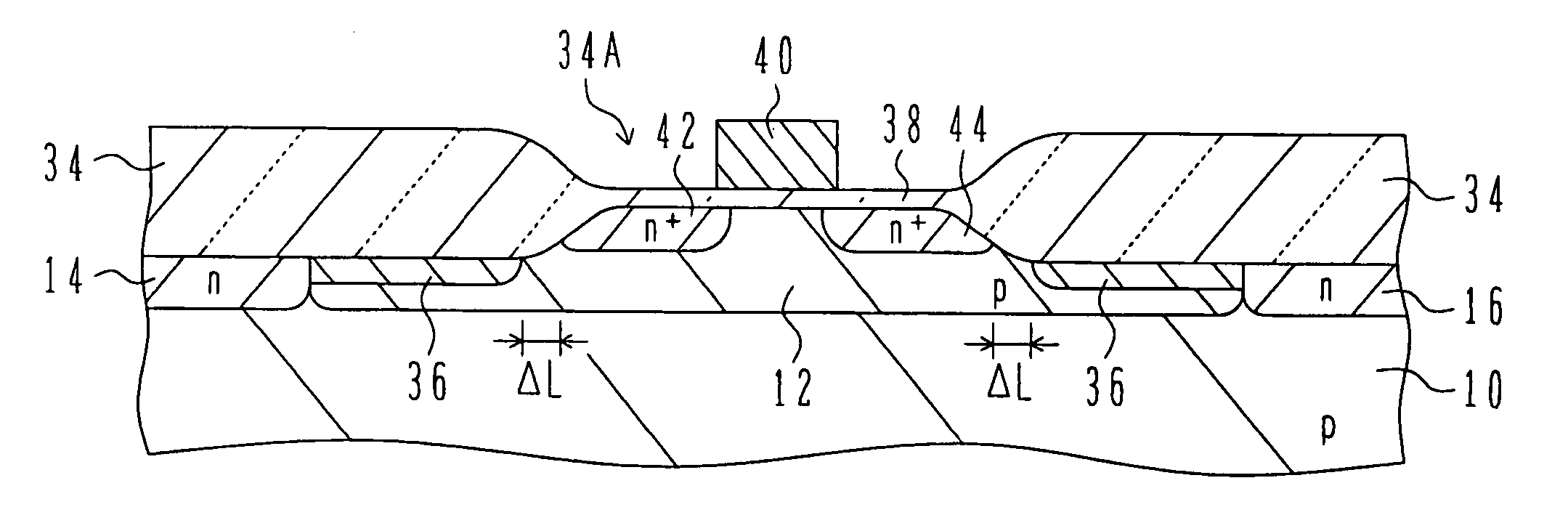
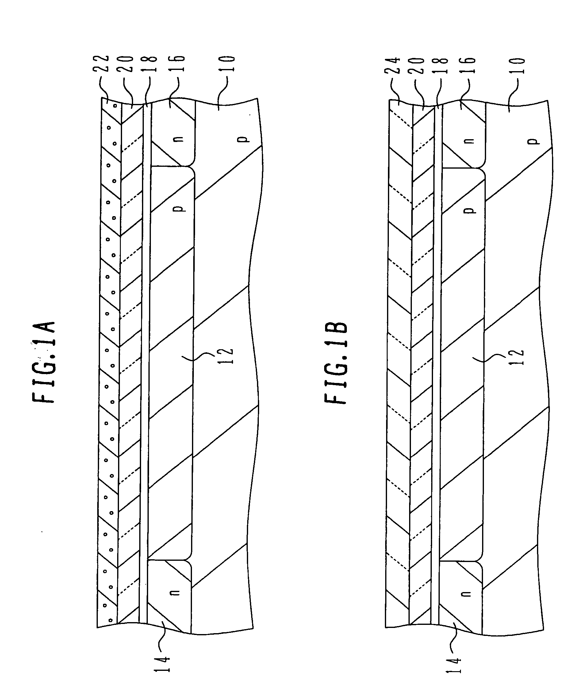
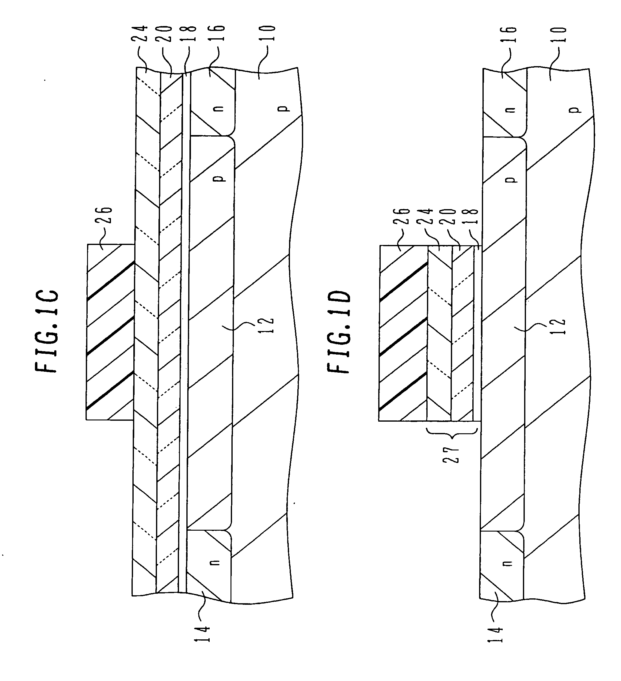
[0069]FIGS. 1A to 1J illustrate a manufacture method for a metal oxide semiconductor (MOS) type integrated circuit (IC) using a field oxide film forming method according to the present invention. Processes corresponding to FIGS. 1A to 1J will be described sequentially.

[0070] In a process shown in FIG. 1A, a p-type well region 12 and n-type well regions 14 and 16 are formed side by side on a principal surface of a p-type silicon substrate 10 by a well-known method. The n-type well regions 14 and 16 may be formed as one well region surrounding the p-type well region 12. After the well regions 12 to 16 are formed, a silicon oxide film (stress relaxing pad oxide film) 18 is formed on the principal surface of the substrate 10 by thermal oxidation. A thickness of the silicon oxide film 18 may be, for example, in a range from 30 nm to 40 nm. A silicon nitride film 20 is formed on the silicon oxide film 18 by CVD, and a polysilicon film 22 is formed on the silicon nitride film 20 by CVD. A ...

second embodiment

[0100]FIGS. 3A to 3H illustrate a manufacture method for an n-channel MOS type transistor of a complementary metal oxide semiconductor (CMOS) type IC according to the present invention. Processes corresponding to FIGS. 3A to 3H will be described sequentially.

[0101] In a process shown in FIG. 3A, a p-type well region 112 and n-type well regions 114 and 116 are formed side by side on a principal surface of a p-type silicon substrate 110 by a well-known method. The n-type well regions 114 and 116 may be formed as one well region surrounding the p-type well region 112. After the well regions 112 to 116 are formed, a silicon oxide film (stress relaxing pad oxide film) 118 is formed on the principal surface of the substrate 110 by thermal oxidation. A thickness of the silicon oxide film 118 may be, for example, in a range from 30 nm to 40 nm. A silicon nitride film 120 is formed on the silicon oxide film 118 by CVD. A thickness of the silicon nitride film 120 may be 75 nm to 150 nm (prefe...


PUM


Abstract

On the principal surface of a silicon substrate, a side spacer made of silicon nitride is formed on the side wall of a lamination including a silicon oxide film, a silicon nitride film and a silicon oxide film. Thereafter, a channel stopper ion doped region is formed by implanting impurity ions by using as a mask the lamination, side spacer and resist layer. After the resist layer and side spacer are removed, a field oxide film is formed through selective oxidation using the lamination as a mask, and a channel stopper region corresponding to the ion doped region is formed. After the lamination is removed, a circuit device such as a MOS type transistor is formed in each device opening of the field oxide film.

Description

CROSS REFERENCE TO RELATED APPLICATION [0001] This application is based on and claims priority of Japanese Patent Applications No. 2005-028699 filed on Feb. 4, 2005 and No. 2005-078628 filed on Mar. 18, 2005, the entire contents of which are incorporated herein by reference. BACKGROUND OF THE INVENTION [0002] A) Field of the Invention [0003] The present invention relates to a method of forming a field oxide film (isolation film) suitable for the manufacture of a metal oxide semiconductor (MOS) type integrated circuit (IC), and more particularly to techniques of forming a channel stopper region just under the field oxide film and spaced apart from a device opening. [0004] B) Description of the Related Art [0005] A method of utilizing side spacers as illustrated in FIGS. 7A to 7C is known as a conventional method of forming a field oxide film with a channel stopper region just under the filed oxide film and spaced apart from the device opening (for example, refer to JP-A-HEI-5-136123)...

Claims


Application Information

Patent Timeline
IPC IPC(8): H01L21/425
CPCH01L29/0638H01L29/78H01L21/18H01L21/76
Inventor TAKAMI, SYUUSEIFUKAMI, HIROAKI
Owner YAMAHA CORP
Why Eureka
Try Eureka