Method and apparatus for testing, characterizing and monitoring a chip interface using a second data path

a chip interface and data path technology, applied in the field of digital data processing, can solve problems such as uneven degradation of signals received by receiving chips, add more layers of complexity to a system, and degrade the signal of receiving chips

Inactive Publication Date: 2006-08-24
LENOVO GLOBAL TECH INT LTD
View PDF2 Cites 33 Cited by
  • Summary
  • Abstract
  • Description
  • Claims
  • Application Information

AI Technical Summary

Benefits of technology

[0025] A characterizable interface in accordance with the preferred embodiment of the present invention supports the accurate determination of low frequency intermittent errors on an individual line basis for a plurality of signal delay settings. Characterization can be accomplished under realistic operating conditions when data associated with an application program is transmitted across the inter-chip communication lines. Systems designers may therefore test, characterize, and monitor the inter-chip interfaces on an individual line basis after the chips and the circuit boards to which they are mounted have been designed and constructed. While the primary benefit is assumed to be understanding the interface in the system design phase, such capability could further be used to test, characterize and monitor chips during manufacturing to account for manufacturing variations, or in the field to account for variations in operating environment, aging, and so forth.

Problems solved by technology

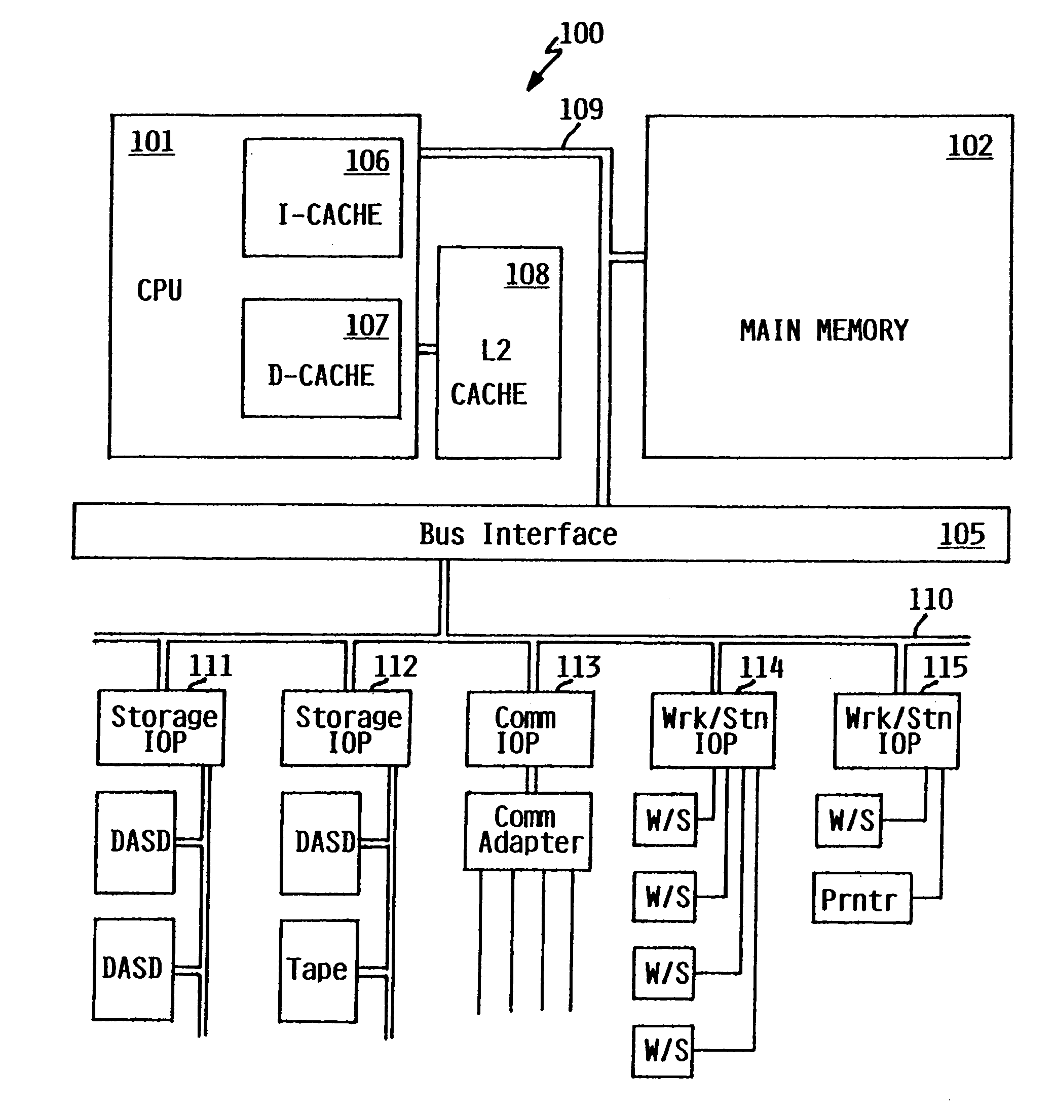
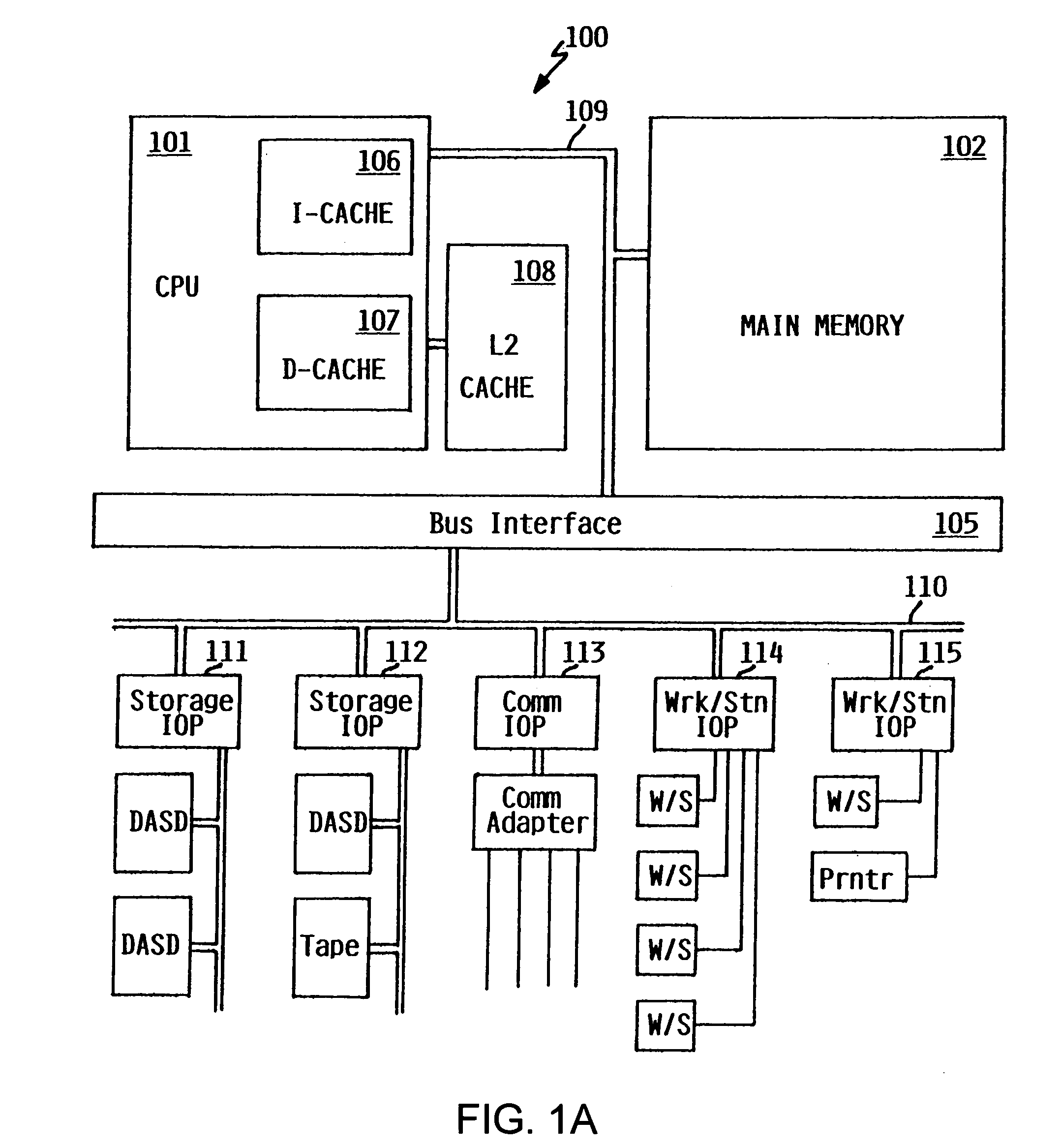
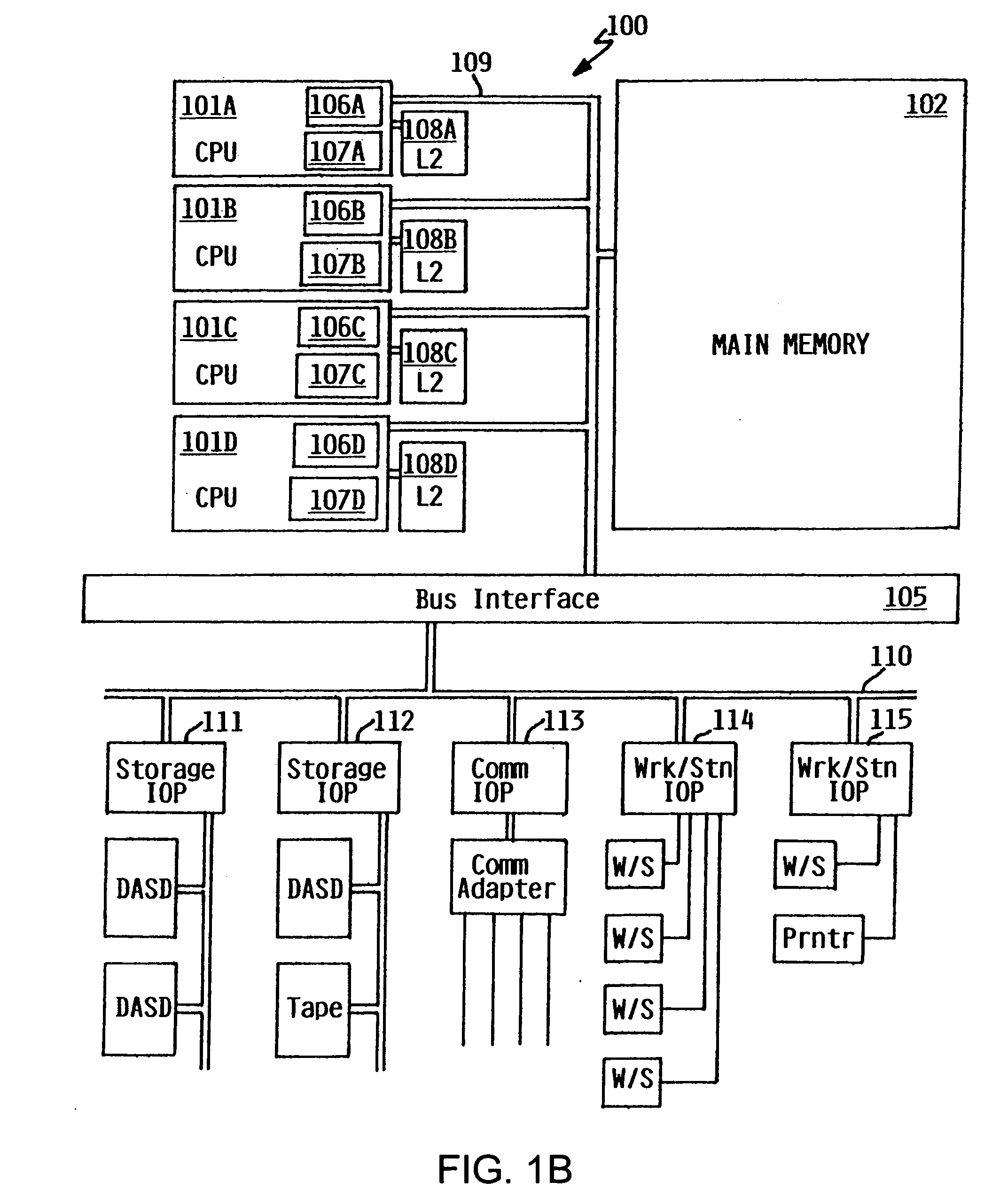
Early computer processors, which were constructed from many discrete components, were susceptible to significant speed improvements by shrinking component size, reducing component number, and eventually, packaging the entire processor as an integrated circuit on a single chip.
The modest cost of individual processors packaged on integrated circuit chips has made multi-processor systems practical, although such multiple processors add more layers of complexity to a system.
Where numerous inter-chip communication lines connect multiple ports on multiple chips, all simultaneously communicating data, various factors can degrade the signals received by a receiving chip.
This degradation is not uniform.
It is therefore inevitable that some lines will exhibit a greater signal degradation, and will be more prone to soft (i.e., intermittent, non-repeatable) errors, than others.
Random variations in the signal have many possible causes too numerous to mention, but in general certain conditions make a line more susceptible to variation, such as physical length of the line, the strength of the drivers, etc.
However, slowing the clock signal to accommodate the worst case signal line may adversely affect system throughput.
As the number of signal lines increases, the variation of the worst case line is likely to be more extreme, requiring further slowing of the clock.
As the number and density of lines increases, connecting test probes to individual lines is increasingly difficult and time consuming.
When transmission errors are of an intermittent and infrequent nature, such conventional testing equipment is often inadequate to the task of characterizing the interface.
Tuning elastic interfaces according to these techniques is a time-consuming process, which only promises to become more difficult as the number of inter-chip communication lines increases in future designs.
Moreover, such tuning does not necessarily take other signal degrading factors into account, including signal degrading factors that occur in the field when the system is installed and placed in service after having been designed, and does not necessarily obtain optimal results.
These fluctuations and the sensitivity of the links can create problems when designing, manufacturing, installing and using multi-node systems.
Moreover, link errors are also impacted by the type of data being sent across the link.
Consequently, merely checking for errors in the link using one type of data, e.g., using random data, is not a good predictor of the performance of the link for other types of data.
For example, if data associated with an application program being run by the system is transmitted across the link instead of random data, link errors could increase or decrease.
Similarly, if the application program being run by the system changes, link errors could increase or decrease.
If the comparison results in a miscompare, then the packet was not transmitted and received successfully and an error is logged.
A problem with the ping test is that it is a point test, i.e., tuning parameters such as signal delay are not varied.
In addition, because the ping test checks for errors in the link using one type of data, i.e., using random data, the ping test in not a good predictor of the performance of the link for other types of data.
For example, if data associated with an application program subsequently run by the system is transmitted across the link instead of random data, the error rate of the link could increase or decrease.
However, running the bathtub curve test requires bringing the system down because clocks must be stopped in the chips to read and set data.
In addition, because construction of a bathtub curve according to current techniques checks for errors in the link using one type of data, i.e., using random data, the ping test is not a good predictor of the performance of the link for other types of data.
For example, if data associated with an application program subsequently run by the system is transmitted across the link instead of random data, the error rate of the link could increase or decrease.

Method used


Image

  • Method and apparatus for testing, characterizing and monitoring a chip interface using a second data path
  • Method and apparatus for testing, characterizing and monitoring a chip interface using a second data path
  • Method and apparatus for testing, characterizing and monitoring a chip interface using a second data path

Examples


Embodiment Construction

[0041] Referring to the Drawing, wherein like numbers denote like parts throughout the several views, FIG. 1A is a high-level representation of the major hardware components of a single-CPU computer system 100 for utilizing an inter-chip interface, according to the preferred embodiment of the present invention. CPU 101 processes instructions and data from main memory 102. CPU 101 temporarily holds instructions and data in a cache structure for more rapid access. In the embodiment of FIG. 1A, the cache structure is shown as separate internal level one instruction cache 106 (L1 I-cache) and level one data cache 107 (L1 D-cache), and level two cache 108 (L2 cache) closely coupled to CPU 101. However, it should be understood that the cache structure may be different; that the number of levels and division of function in the cache may vary; and that a system might in fact have no cache at all. L1 I-cache 106 stores instructions for execution by CPU 101. L1 D-cache 107 stores data (other ...


PUM


Abstract

A data receiver circuit in a receiving chip provides the capability to characterize an interface, which includes one or more inter-chip communication lines, between a transmitting chip and the receiving chip by transmitting the data across a primary data path and a secondary data path, latching the data in the secondary data path using a clock signal that is skewed relative to a clock signal used to latch the primary data path, comparing the data latched from the primary and secondary data paths, and recording errors. Because the primary data path is not impacted by the test cycle, the test cycle may be run while data associated with applications running on the system are transmitted across the inter-chip communication lines.

Description

BACKGROUND OF THE INVENTION [0001] 1. Field of Invention [0002] The present invention relates in general to the digital data processing field. More particularly, the present invention relates to testing, characterizing and monitoring chip interfaces for communicating data between integrated circuit chips. [0003] 2. Background Art [0004] In the latter half of the twentieth century, there began a phenomenon known as the information revolution. While the information revolution is a historical development broader in scope than any one event or machine, no single device has come to represent the information revolution more than the digital electronic computer. The development of computer systems has surely been a revolution. Each year, computer systems grow faster, store more data, and provide more applications to their users. [0005] A modern computer system typically comprises a central processing unit (CPU) and supporting hardware necessary to store, retrieve and transfer information, ...

Claims


Application Information

Patent Timeline
Patent Type & Authority Applications(United States)
IPC IPC(8): G06F3/06
CPCG06F11/24
Inventor ALDEREGUIA, ALFREDOKOEHLER, BRIAN LEERICHTER, GRACE ANN
Owner LENOVO GLOBAL TECH INT LTD
Why Eureka
Try Eureka