Non-volatile and static random access memory cells sharing the same bitlines

a random access memory and non-volatile technology, applied in static storage, information storage, digital storage, etc., can solve the problems of non-volatile semiconductor memory being typically slower to operate than volatile memory, sram is typically more expensive to manufacture than dram, loss of data, etc., to achieve faster total data transfer time, more power efficiency, and faster total transfer time

Inactive Publication Date: 2006-08-31
O2IC
View PDF58 Cites 61 Cited by
  • Summary
  • Abstract
  • Description
  • Claims
  • Application Information

AI Technical Summary

Benefits of technology

[0023] A multitude of the memory structures of the present invention may be used to form an array. The multitude of memory structures may be connected to the same wordline by connecting their first input terminals to that wordline. Accordingly, the multitude of memory structures may perform the loading of data to their associated SRAM cells from their associated non-volatile memory cells via their respective bitlines concurrently. As a result, the total data transfer time from the non-volatile memory cells to their associated SRAM cells when the SRAM cells are loaded concurrently is shorter than when the SRAM cells are loaded individually. In addition, as a consequence of the faster total transfer time, the concurrent loading of the SRAM cells may be more power efficient than if the SRAM cells were to be loaded individually.
[0024] In accordance with the present invention, since the non-volatile and the SRAM memory cells of each memory structure share the same pair of bitlines, data may be loaded from the SRAM cells to their associated non-volatile memory cells via their respective pair of bitlines concurrently. The total transfer time from the SRAM cells to the nonvolatile memory cells when the nonvolatile memory cells are loaded concurrently is shorter than when the nonvolatile memory cells are loaded individually. In addition, as a consequence of the faster total data transfer time, the concurrent loading of non-volatile memory cells may be more power efficient than if the non-volatile memory cells were to be loaded individually.

Problems solved by technology

Due to its larger memory cell size, an SRAM is typically more expensive to manufacture than a DRAM.
Therefore, where loss of data due to power failure or termination is unacceptable, a non-volatile memory is used to store the data.
Unfortunately, a non-volatile semiconductor memory is typically slower to operate than a volatile memory.
Furthermore, the non-volatile memory often requires a high voltage, e.g., 12 volts, to program or erase.
Such high voltages may cause a number of disadvantages.
The high voltage increases the power consumption and thus shortens the lifetime of the battery powering the memory.
The high voltage may degrade the ability of the memory to retain its charges due to hot-electron injection.
The high voltage may cause the memory cells to be over-erased during erase cycles.
Cell over-erase results in faulty readout of data stored in the memory cells.
Unfortunately, most of the portable electronic devices may still require at least two devices, including the non-volatile and volatile, to carry out backup operations.
Two devices are often required since each of the devices often rely on different process technologies, which are often incompatible with each other.
One disadvantage of using two separate devices, including non-volatile and volatile devices, is the data transfer from one device to another.
If there is a lot of data that needs to be transferred from one device to another, and if the data bus width between the two devices is small compared to the amount of data to be transferred, then the data transfer may suffer from long transfer times. In addition, long transfer times may also result in a large power consumption, which is undesirable when battery life is limited.
The cumulative data transfer time may thus be undesirably long and the total power consumed may be undesirably too large.
In addition, if a CPU is required to transfer data between the non-volatile and volatile devices, then the total amount of time spent transferring data will have an adverse impact on the CPU's ability to perform other tasks.
SRAM 40 consumes relatively large amount of power and occupies a relative large semiconductor surface area.

Method used


Image

  • Non-volatile and static random access memory cells sharing the same bitlines
  • Non-volatile and static random access memory cells sharing the same bitlines
  • Non-volatile and static random access memory cells sharing the same bitlines

Examples


Embodiment Construction

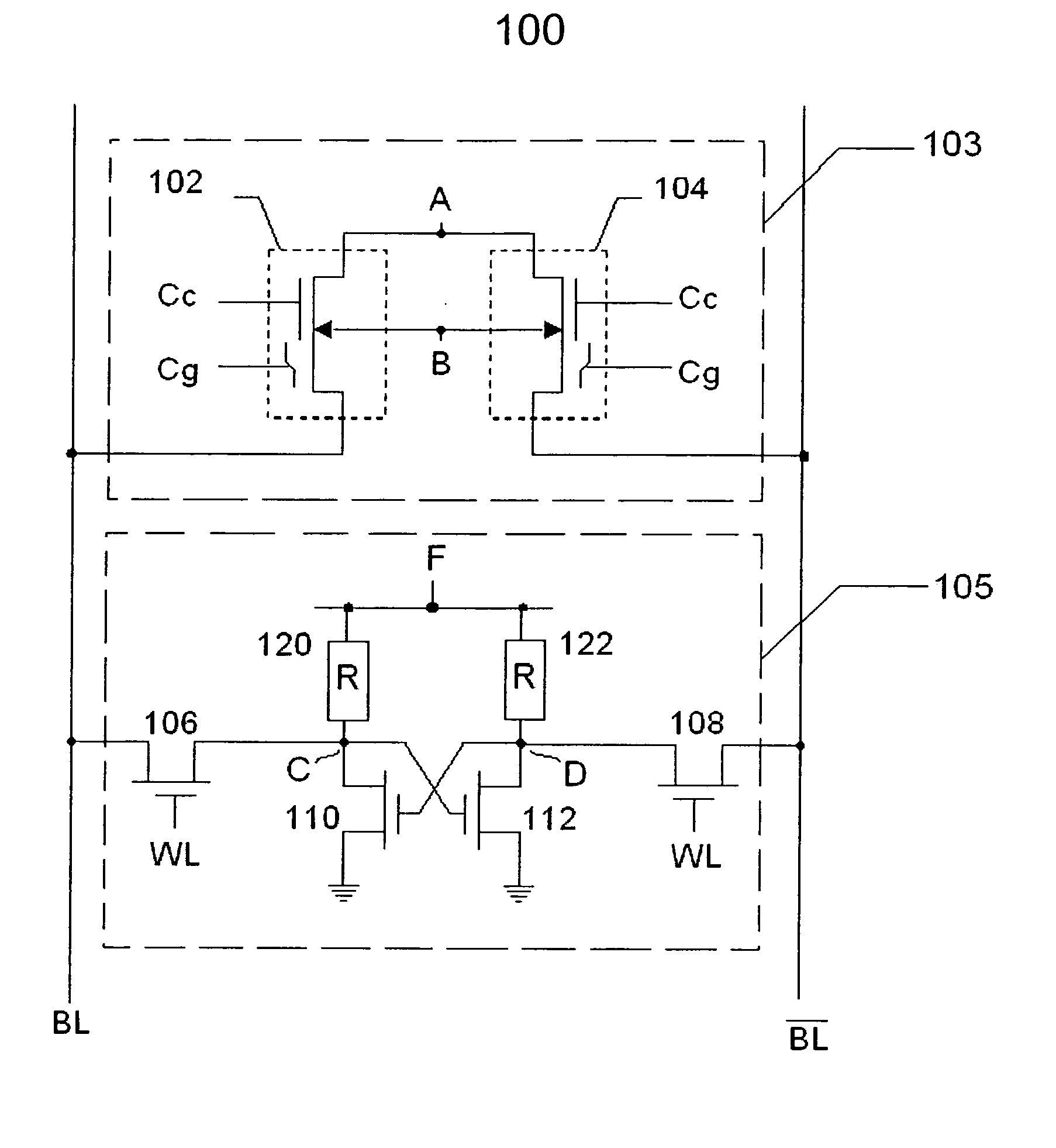
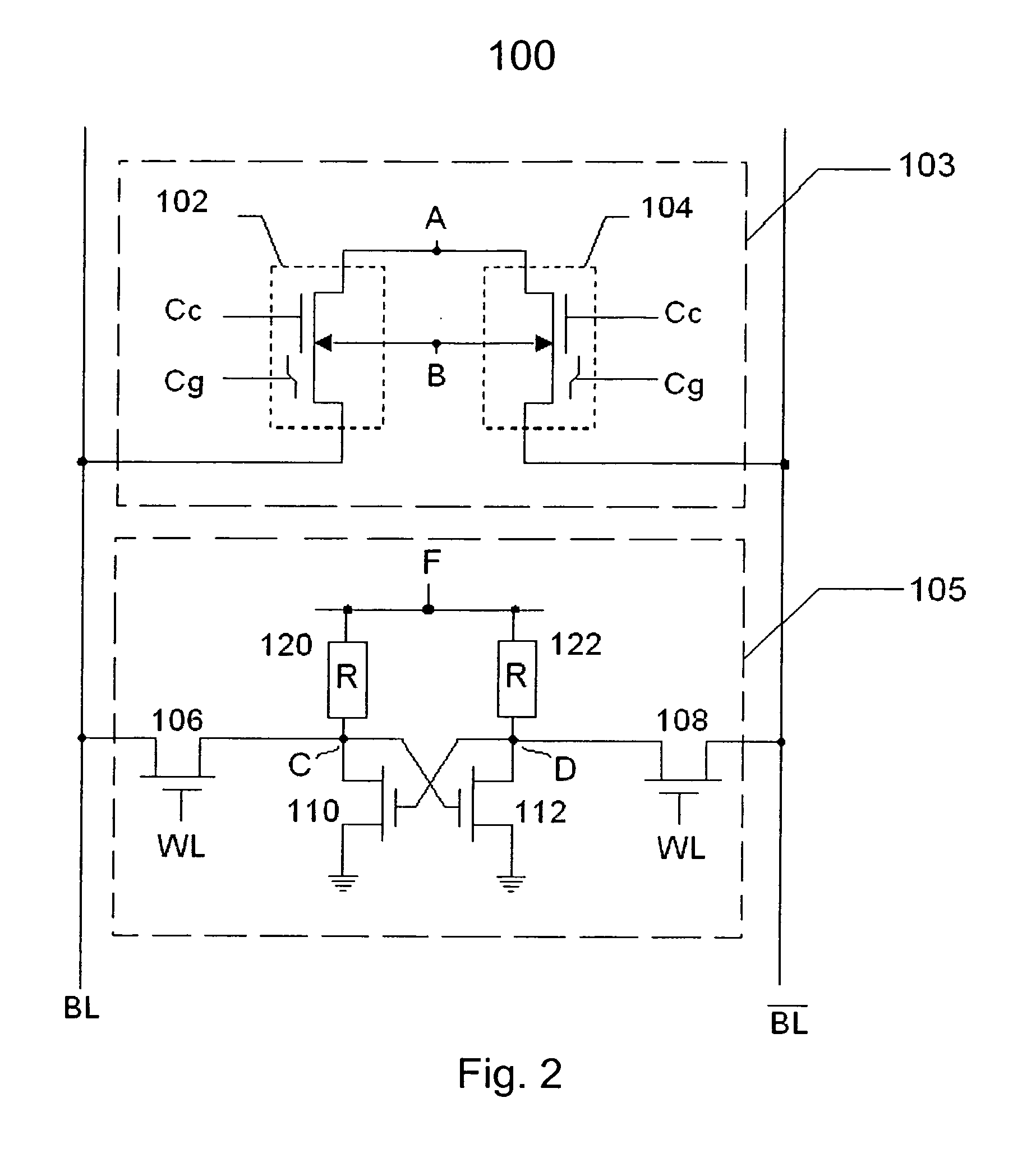
[0037] According to the present invention, an improved memory structure and method is provided. More particularly, the invention provides a semiconductor memory that has integrated non-volatile and static random access memory cells structures sharing the same bitlines. Although the invention has been applied to a single integrated memory structure in a memory application, there can be other alternatives, variations, and modifications. For example, the invention can be applied to embedded memory applications, including those with logic or microcircuits, and the like.

[0038]FIG. 2 is a transistor schematic diagram of an integrated memory structure 100 that operates differentially and includes both non-volatile memory cells and an SRAM cell, in accordance with one embodiment of the present invention. This diagram is merely an example, which should not unduly limit the scope of the claims herein. One of ordinary skill in the art would recognize many other variations, modifications, and ...


PUM


Abstract

A memory cell structure includes non-volatile as well as SRAM memory cells that share the same bitline and operate differentially. The SRAM cell includes first and second MOS transistors that are coupled to the same true and complementary bit lines that the non-volatile memory cells are coupled to. The non-volatile memory cells are erased prior to being programmed. Programming of the non-volatile memory cells may be carried out via hot-electron injection or Fowler-Nordheim tunneling. Data stored in the non-volatile memory cells may be transferred to the SRAM cell. The differential reading and writing of data reduces over-erase of the non-volatile devices.

Description

CROSS-REFERENCES TO RELATED APPLICATIONS [0001] The present application is related to copending application Ser. No. 10 / 394,417, entitled “Non-Volatile Memory Device,” filed Mar. 19, 2003, Attorney Docket No. 021801-000210US, assigned to the same assignee, and incorporated herein by reference in their entirety.BACKGROUND OF THE INVENTION [0002] The present invention relates to semiconductor integrated circuits. More particularly, the invention provides a semiconductor memory structure that has integrated non-volatile and static random access memory cells. Although the invention has been applied to a single integrated memory structure in a memory application, there can be other alternatives, variations, and modifications. For example, the invention can be applied to embedded memory applications, including those with logic or micro circuits, and the like. [0003] Semiconductor memory devices have been widely used in electronic systems to store data. There are generally two types of mem...

Claims


Application Information

Patent Timeline
Patent Type & Authority Applications(United States)
IPC IPC(8): G11C11/34G11C14/00
CPCG11C14/00
Inventor CHOI, DAVID S.KWON, EUI PILCHOI, KYU HYUN
Owner O2IC
Why Eureka
Try Eureka