Semiconductor light-emitting device

a technology of light-emitting devices and semiconductors, which is applied in the direction of heat exchangers, heat exchangers, and semiconductor lasers, can solve the problems of insufficient differential efficiency of semiconductor light-emitting devices, and achieve the effect of higher differential efficiency

Active Publication Date: 2006-08-31
MITSUBISHI ELECTRIC CORP
View PDF8 Cites 251 Cited by
  • Summary
  • Abstract
  • Description
  • Claims
  • Application Information

AI Technical Summary

Benefits of technology

[0009] It is an object of the present invention to provide a semiconductor light-emitting device using a Group III-V nitride compound semiconductor and having differential efficiency higher than conventional ones.

Problems solved by technology

This has rendered semiconductor light-emitting devices having sufficiently high differential efficiency unobtainable.

Method used


Image

  • Semiconductor light-emitting device
  • Semiconductor light-emitting device
  • Semiconductor light-emitting device

Examples


first preferred embodiment

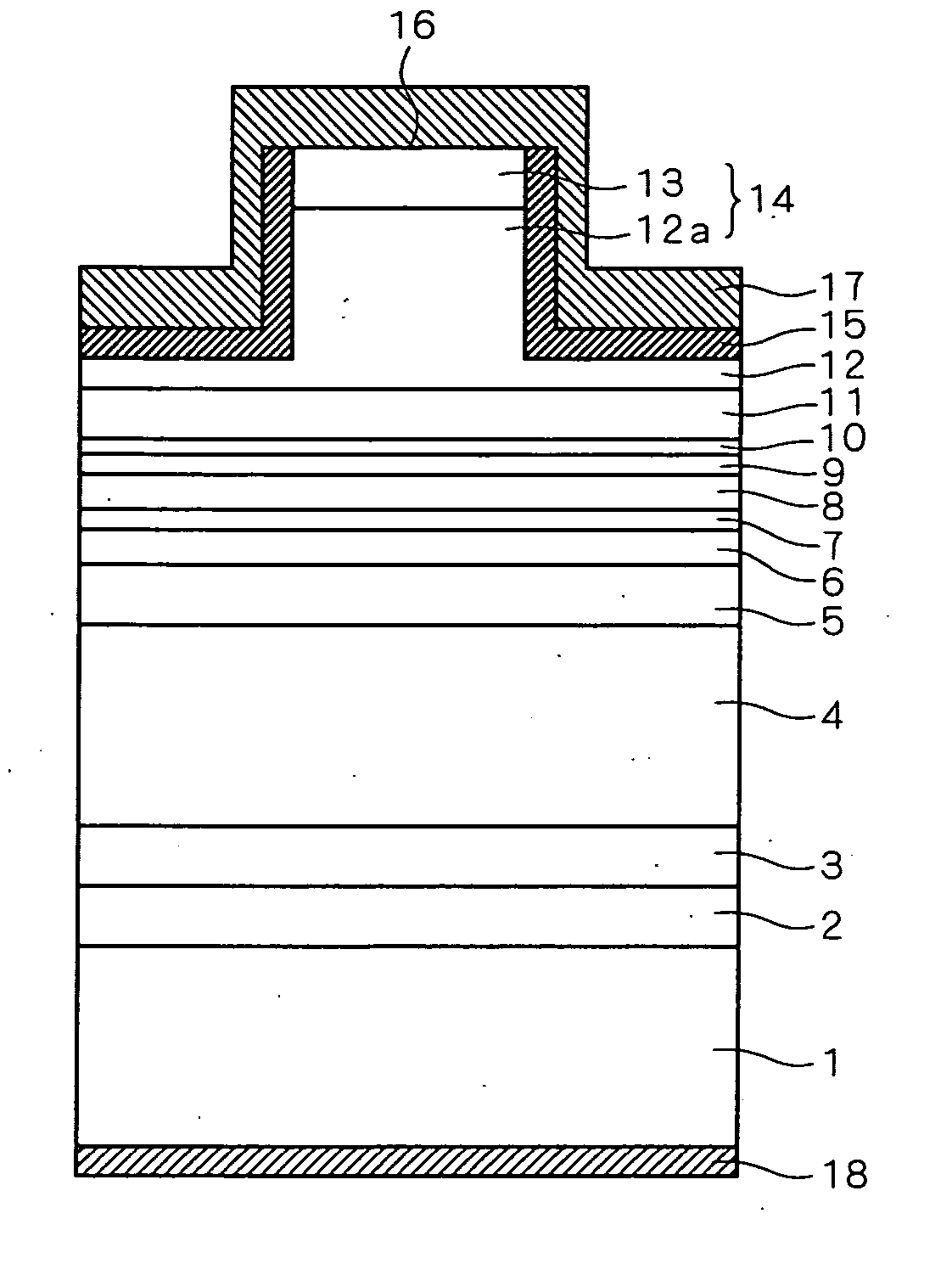
[0061]FIG. 7 is a cross-sectional view illustrating the structure of a semiconductor laser (semiconductor light-emitting device) using the Group III-V nitride compound semiconductors according to a first preferred embodiment of the present invention. This semiconductor laser has a ridge structure and an SCH (Separate Confinement Heterostructure).

[0062] As shown, the semiconductor laser according to the first preferred embodiment has an n-type GaN buffer layer 2 formed on a Ga surface, namely one main surface, of a GaN substrate 1. The n-type GaN buffer layer 2 is employed in order to reduce the unevenness of the one main surface of the GaN substrate 1 so that layers can be laminated thereon as evenly as possible.

[0063] An n-type AlGaN cladding layer 3 having an Al composition ratio of 0.07, an n-type AlGaN cladding layer 4 having an Al composition ratio of 0.045, and an n-type AlGaN cladding layer 5 having an Al composition ratio of 0.015 are laminated in order on the n-type GaN b...

second preferred embodiment

[0110] Table 3 indicates the material, thickness and refractive index “n” of each layer forming a semiconductor laser according to a second preferred embodiment of the present invention. The layer numbers in the leftmost column of Table 3 correspond to the reference numbers of the layers in the FIG. 7 structure.

TABLE 3LayerRefractiveNo.Layer NameMaterialThicknessIndex “n”13contact layerp-GaN 20 nm2.46712cladding layerp-Al0.07Ga0.93N 500 nm2.501311guide layerp-GaN 100 nm2.46710electron barrier layerp-Al0.2Ga0.8N 20 nm2.42579SCH layerIn0.02Ga0.98N 30 nm2.57118well layerIn0.14Ga0.86N  3.5 nm2.765barrier layerIn0.02Ga0.98N  7.0 nm2.5711well layerIn0.14Ga0.86N  3.5 nm2.765barrier layerIn0.02Ga0.98N  7.0 nm2.5711well layerIn0.14Ga0.86N  3.5 nm2.7657SCH layerIn0.02Ga0.98N 30 nm2.57116guide layern-GaN 80 nm2.4675cladding layern-Al0.015Ga0.985N 330 nm2.53644cladding layern-Al0.045Ga0.955N1000 nm2.51733cladding layern-Al0.07Ga0.93N 400 nm2.50131GaN substraten-GaN2.467

[0111] As shown in Tabl...

third preferred embodiment

[0115]FIG. 13 is a cross-sectional view illustrating the structure of a semiconductor laser using the Group III-V nitride compound semiconductors according to a third preferred embodiment of the present invention. As shown, this semiconductor laser has the same layer structure as that of the first preferred embodiment illustrated in FIG. 7, except that the three n-type AlGaN cladding layers 3 to 5 are replaced with one n-type AlGaN cladding layer 20, and the p-type AlGaN cladding layer 12 is replaced with a p-type AlGaN cladding layer 21.

[0116] Table 4 indicates the material, thickness and refractive index “n” of each layer forming the semiconductor laser corresponding to the third preferred embodiment. The layer numbers in the leftmost column of Table 4 correspond to the reference numbers of the layers in the FIG. 13 structure.

TABLE 4LayerRefractiveNo.Layer NameMaterialThicknessIndex “n”13contact layerp-GaN 20 nm2.46721cladding layerp-Al0.03Ga0.97N 570 nm2.526911guide layerp-GaN...


PUM


Abstract

In a semiconductor laser having an active layer of double-quantum-well structure that includes two InGaN well layers each of which has a thickness of 5 nm, a threshold current deteriorates to a relatively small degree while differential efficiency is improved considerably in a region having a light confinement coefficient Γ of 3.0% or less. On the other hand, with the light confinement coefficient Γ becoming less than 1.5%, the threshold current increases considerably while the amount of improvement in differential efficiency becomes small. It is therefore preferable that the lowest limit to the light confinement coefficient Γ be about 1.5%. The differential efficiency of 1.6 W/A or more is obtained with the light confinement coefficient Γ being 3.0% or less, and the differential efficiency of 1.7 W/A or more is obtained with the light confinement coefficient Γ being 2.6% or less.

Description

BACKGROUND OF THE INVENTION [0001] 1. Field of the Invention [0002] The present invention relates to semiconductor light-emitting devices such as semiconductor lasers and light-emitting diodes using Group III-V nitride compound semiconductors. [0003] 2. Description of the Background Art [0004] As semiconductor lasers capable of light emission over a region ranging from blue to ultraviolet that is necessary for greater density of optical disc, research and development has been actively conducted in recent years on nitride semiconductor lasers using Group III-V nitride compound semiconductors such as AlGaInN, which have been put to practical use. [0005] Nitride semiconductor lasers reported to date have, as their active layer structure, a multi-quantum-well structure in which a well layer made of InGaN (InGaN well layer) and a barrier layer made of InGaN (InGaN barrier layer) and having a lower In composition ratio (commonly about 0.02) than the well layer are alternately laminated. A...

Claims


Application Information

Patent Timeline
Patent Type & Authority Applications(United States)
IPC IPC(8): H01S5/20H01S5/00H01S5/323B82Y20/00H01S5/343
CPCB82Y20/00H01S5/20H01S5/2004H01S5/2009H01S5/22H01S5/34333A61H33/063A61H2033/061A61H2201/0169A61H2201/0228H05B3/06
Inventor KURAMOTO, KYOSUKE
Owner MITSUBISHI ELECTRIC CORP
Why Eureka
Try Eureka