Increased light extraction from a nitride LED

Inactive Publication Date: 2006-09-14
GELCORE LLC (US)
View PDF19 Cites 97 Cited by
  • Summary
  • Abstract
  • Description
  • Claims
  • Application Information

AI Technical Summary

Problems solved by technology

A problem can arise in the flip-chip configuration when the growth substrate is substantially light-absorbing over some or all of the spectral range of light emission.
Moreover, even if a suitable optically transparent substrate is available, such as is the case for group III-nitride light emitting diodes which can be grown on transparent sapphire, optical reflective losses can occur at the interface between the substrate and the epitaxial layers due to an abrupt discontinuity in refractive index.
As a result, while the removal of the sapphire substrate from a n

Method used


Image

  • Increased light extraction from a nitride LED
  • Increased light extraction from a nitride LED
  • Increased light extraction from a nitride LED

Examples


Example

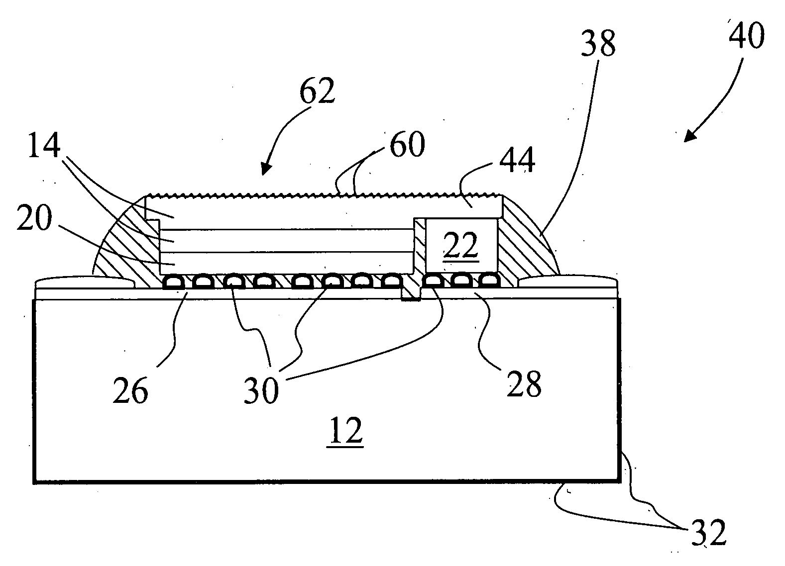
[0015] With reference to FIG. 1, a light emitting die 10 is mounted in flip-chip fashion on a mount or submount wafer 12. The die 10 includes a semiconductor device layers stack 14 that is epitaxially deposited on a growth substrate 16. The epitaxial device layers stack 14 can comprise a group III nitride ultraviolet or blue light material, a group III phosphide visible-emission material, or the like.

[0016] The semiconductor layers stack 14 is depicted with two exemplary layers corresponding to a simple p / n diode; however, those skilled in the art will appreciate that more complex semiconductor layer stack can be employed. For a group III nitride ultraviolet or blue light emitting diode with a p-on-n orientation, the layers stack typically includes an epitaxial growth buffer of aluminum nitride or another material, an n-type gallium nitride base layer, an active region of indium gallium nitride, a p-type gallium nitride layer, and optionally a contact layer formed on the p-type gal...


PUM


Abstract

In a method for fabricating a flip-chip light emitting diode device, a submount wafer is populated with a plurality of the light emitting diode dies. Each device die is flip-chip bonded to the submount. Subsequent to the flip-chip bonding, a growth substrate is removed. The entire submount is immersed in the etchant solution, exposed to the light for a prespecified period of time, removed from the solution, dried and diced into a plurality of LEDs., The LEDs are immediately packaged without any further processing.

Description

BACKGROUND [0001] The present application relates to the electronics arts. It particularly relates to group III-nitride flip-chip bonded light emitting diodes for lighting applications, and will be described with specific reference thereto. However, it also finds application in conjunction with other types of flip-chip bonded epitaxial semiconductor devices, and the like. [0002] In a flip-chip mounting configuration, a light emitting diode with a light-transmissive substrate and front-side electrodes is bonded “face down” to bonding bumps of a mount, that is, with the epitaxial layers proximate to the mount and a light-transmissive substrate distal from the mount. The flip-chip arrangement has a number of advantages, including improved thermal heat sinking due to the proximity of the active layers to the submount, and reduction of electrode shadowing losses. [0003] In the flip-chip mounting configuration, light is extracted from the substrate side. For epitaxially grown light emitti...

Claims


Application Information

Patent Timeline
IPC IPC(8): H01L21/00H01L33/00H01L33/22H01L33/62
CPCH01L33/0079H01L33/22H01L33/62H01L2224/16H01L2924/00014H01L33/0093H01L2224/05644H01L2224/05599H01L2224/0555H01L2224/0556H01L2224/05568H01L2224/05573H01L2224/0554
Inventor SACKRISON, MICHAEL J.VENUGOPALAN, HARI S.GAO, XIANG
Owner GELCORE LLC (US)
Why Eureka
Try Eureka