Barrier layers for conductive features

a technology of barrier layer and conductive feature, which is applied in the direction of semiconductor/solid-state device details, thin material processing, semiconductor devices, etc., can solve the problems of time delay beginning to limit the propagation delay of integrated circuits, conductive features made from these materials have exhibited an increase in propagation delay, and the difficulty of using copper as an interconnect material, etc., to achieve low resistance and increase conductivity

Inactive Publication Date: 2006-09-14
INFINEON TECH AG
View PDF16 Cites 46 Cited by
  • Summary
  • Abstract
  • Description
  • Claims
  • Application Information

AI Technical Summary

Benefits of technology

[0013] Advantages of preferred embodiments of the present invention include providing barrier layers wherein the barrier layer material is different on the sidewalls of trenches than at the top surfaces, inducing larger grain growth ...

Problems solved by technology

However, as semiconductor devices have been scaled down in size, conductive features made from these materials have exhibited an increase in propagation delay.
For example, as minimum feature size decreases, RC time delay begins to limit the propagation delay of integrated circuits.
However, there are some challenges in using copper for ...

Method used


Image

  • Barrier layers for conductive features
  • Barrier layers for conductive features
  • Barrier layers for conductive features

Examples


embodiment 300

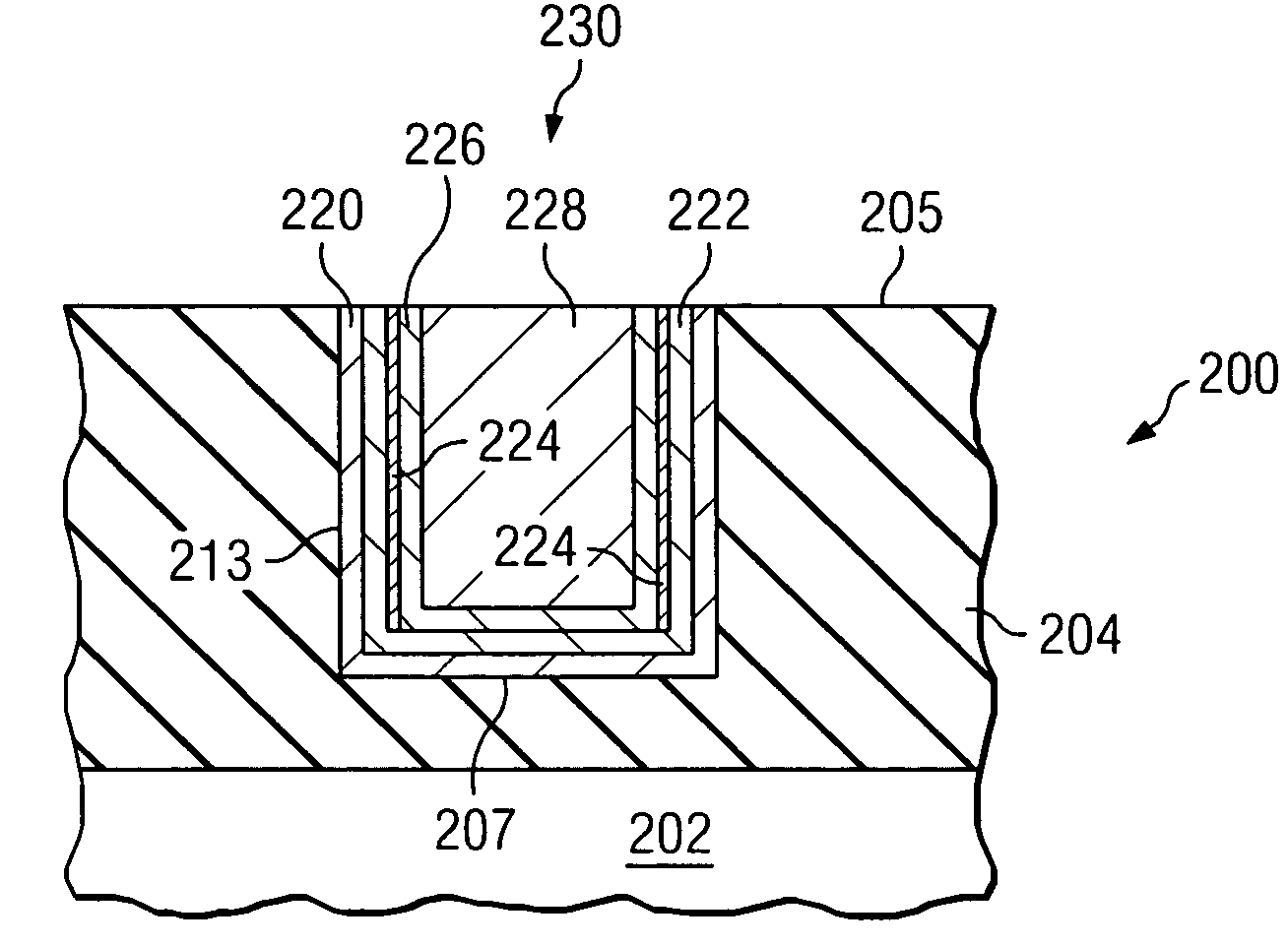
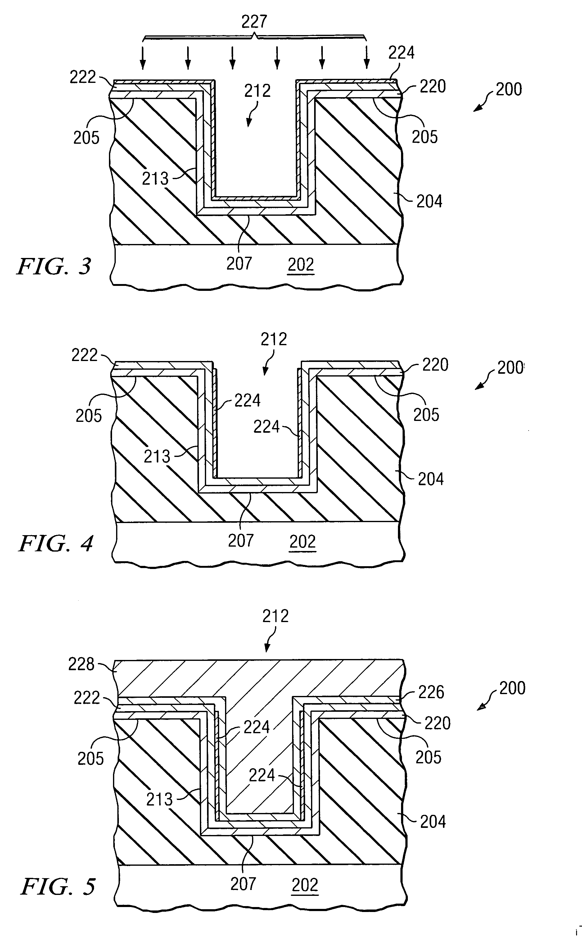
[0044]FIG. 7 shows another embodiment 300 of the present invention. Like numerals are used in FIG. 7 as were used in the embodiment shown in FIGS. 3 through 6. In this embodiment, a highly directional layer 340 of TaN in a hexagonal phase is formed only on the trench 312 bottom surface 307 and the insulating material 304 top surface 305, but not on the sidewalls 313 of the trenches 312. The directional layer 340 of TaN may be formed only on the planar top surfaces 305 and the trench bottom surfaces 307 of the insulating material 304 by adjusting the properties of the deposition technique, for example. A relatively conformal deposition of a layer of Ta 342a / 342b is then deposited over the exposed sidewalls 313 and over the layer 340 of TaN in the hexagonal phase. The Ta nucleates as low resistive alpha Ta 342a on the top surfaces 305 and the trench bottom surfaces 307, and nucleates as a higher resistive beta Ta 342b on the sidewalls 313 of the trenches 312, as shown. Advantageously,...

embodiment 400

[0046]FIG. 8 shows another embodiment 400 of the present invention. In this embodiment, a relatively conformal layer 450 of TaN in a hexagonal phase is deposited over the trenches 412, over the top surfaces 405 and 407 and also over the sidewalls 413. Then a highly directional deposition process is used to deposit a layer 452 of alpha Ta over only the trench bottom 407 and the top surface 405 of the insulating material 404. The layer 452 is not formed over the sidewalls 413, as shown. Thus, the layer 452 of alpha Ta provides fast grain growth for the top surfaces 405 and 407, and the layer 450 of hexagonal TaN provides slow grain growth on the sidewalls 413, for the subsequently deposited conductive material (not shown in FIG. 8; see FIG. 6).

[0047] The layer 450 of TaN in a hexagonal phase preferably comprises a thickness of about 10 nm or less, and the layer 452 of Ta in an alpha phase preferably comprises a thickness of about 20 nm or less, although alternatively, the layers 450 a...


PUM


Abstract

Barrier layers for conductive features and methods of formation thereof are disclosed. A first barrier material is deposited on top surfaces of an insulating material, and a second barrier material is deposited on sidewalls of the insulating material, wherein the second barrier material is different than the first barrier material. The first barrier material induces grain growth of a subsequently deposited conductive material at a first rate, and the second barrier material induces grain growth of the conductive material at a second rate, wherein the second rate is slower than the first rate.

Description

TECHNICAL FIELD [0001] The present invention relates generally to the fabrication of semiconductor devices, and more particularly to the formation of barrier layers for conductive features of integrated circuits. BACKGROUND [0002] Semiconductor devices are used in a variety of electronic applications, such as personal computers, cell phones, digital cameras, and other electronic equipment, as examples. Semiconductor devices are typically fabricated by sequentially depositing insulating or dielectric layers, conductive layers, and semiconductive layers of material over a semiconductor substrate, and patterning the various layers using lithography to form circuit components and elements thereon. [0003] As technology has progressed, the demand for smaller semiconductor devices with improved performance has increased. A move is being made away from the traditional materials used in the past in semiconductor device designs, in order to meet these demands. For example, in the past, alumin...

Claims


Application Information

Patent Timeline
IPC IPC(8): H01L23/48
CPCH01L21/76843H01L21/76844H01L21/76846H01L21/76873H01L23/53223H01L23/53238Y10T428/24479H01L23/53266H01L2221/1089H01L2924/0002H01L23/53252H01L2924/00
Inventor BARTH, HANS-JOACHIMHOLZ, JUERGEN
Owner INFINEON TECH AG
Why Eureka
Try Eureka