Semiconductor device and manufacturing method thereof

Active Publication Date: 2006-09-14
SEMICON COMPONENTS IND LLC
View PDF40 Cites 34 Cited by
  • Summary
  • Abstract
  • Description
  • Claims
  • Application Information

AI Technical Summary

Benefits of technology

[0017] The invention also provides a method of manufacturing a semiconductor device. The method includes providing a device intermediate having a semiconductor substrate, a first insulation layer disposed on its front surface and a pad electrode disposed on the first insulation layer, forming a first opening in the semiconductor substrate from its back surface so that the first insulation layer is exposed at a bottom of the first opening and that the fist opening has a maximum lateral size thereof in a position closer to the front surface than to the back surface, and removing the exposed first insulation film to form a second opening so that the pad electrode is exposed at a bottom of the second opening and that the second opening has a larger lateral size at the end that is connected to the first opening than at the end that is covered by the pad electrode.
[0017] The invention also provides a method of manufacturing a semiconductor device. The method includes providing a device intermediate having a semiconductor substrate, a first insulation layer disposed on its front surface and a pad electrode disposed on the first insulation layer, forming a first opening in the semiconductor substrate from its back surface so that the first insulation layer is exposed at a bottom of the first opening and that the fist opening has a maximum lateral size thereof in a position closer to the front surface than to the back surface, and removing the exposed first insulation film to form a second opening so that the pad electrode is exposed at a bottom of the second opening and that the second opening has a larger lateral size at the end that is connected to the first opening than at the end that is covered by the pad electrode.
[0016] The invention provides a semiconductor device that includes a semiconductor substrate having a front surface and a back surface and having a first opening penetrating the semiconductor substrate from the back surface to the front surface, a first insulation layer disposed on the front surface of the semiconductor substrate and having a second opening that is connected to the first opening, and a pad electrode disposed on the first insulation layer so as to cover the second opening. The fist opening has its maximum lateral size in a position closer to the front surface than to the back surface, and the second opening has a larger lateral size at the end that is connected to the first opening than at the end that is covered by the pad electrode.
[0016] The invention provides a semiconductor device that includes a semiconductor substrate having a front surface and a back surface and having a first opening penetrating the semiconductor substrate from the back surface to the front surface, a first insulation layer disposed on the front surface of the semiconductor substrate and having a second opening that is connected to the first opening, and a pad electrode disposed on the first insulation layer so as to cover the second opening. The fist opening has its maximum lateral size in a position closer to the front surface than to the back surface, and the second opening has a larger lateral size at the end that is connected to the first opening than at the end that is covered by the pad electrode.

Problems solved by technology

Also there is a problem in step coverage of the second wiring 110.

Method used


Image

  • Semiconductor device and manufacturing method thereof
  • Semiconductor device and manufacturing method thereof
  • Semiconductor device and manufacturing method thereof

Examples


first embodiment

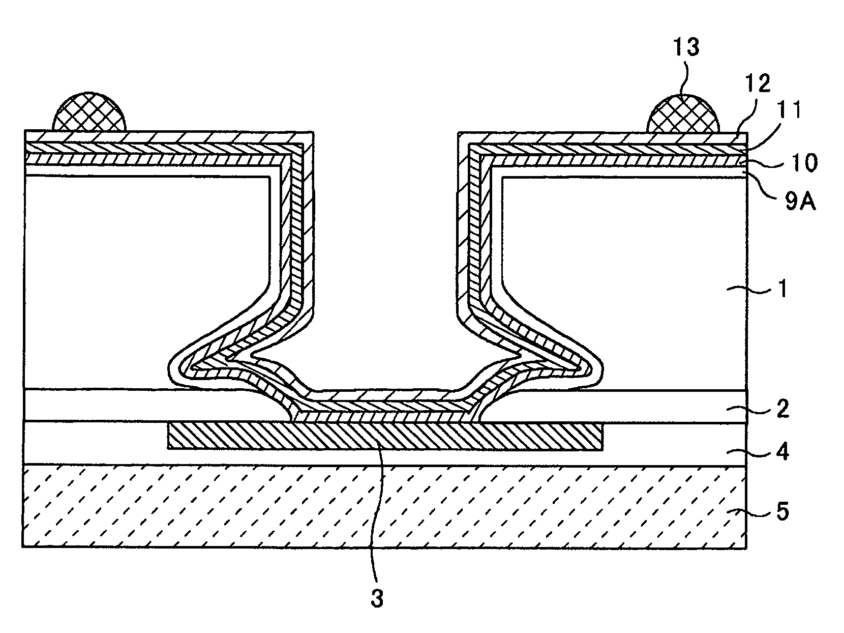
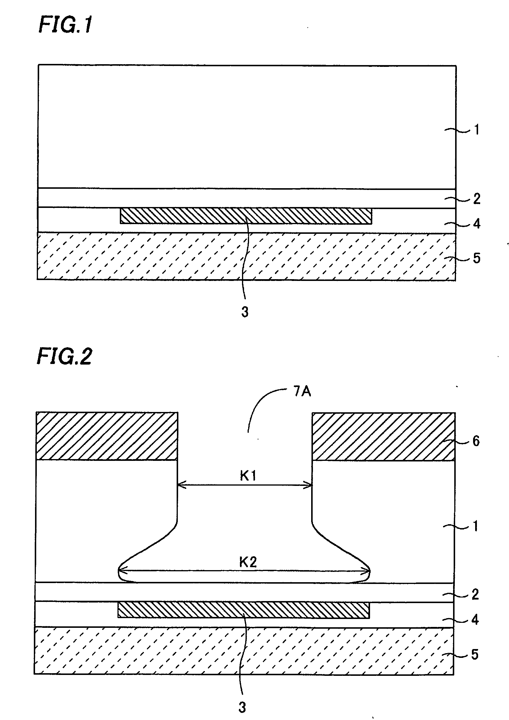
[0025] Next, a semiconductor device according to this invention and its manufacturing method will be described, referring to FIGS. 1-7, which are cross-sectional views showing the semiconductor device applicable to an image sensor and its manufacturing method.

[0026] First, a pad electrode 3 made of aluminum, an aluminum alloy, or copper is formed on the front surface of a semiconductor substrate 1 through a first insulation layer 2 made of, for example, silicon oxide or silicon nitride, as shown in FIG. 1. The pad electrode 3 is connected with a circuit element in a semiconductor die. Then a supporting body 5 such as a glass substrate, a silicon substrate, a plastic substrate, or the like, is bonded to the semiconductor substrate 1 having the pad electrode 3, which is covered with a passivation film made of silicon oxide or silicon nitride, through an adhesive layer 4 made of an epoxy resin. A tape-shaped protective material may be bonded to the semiconductor substrate 1 instead of ...

second embodiment

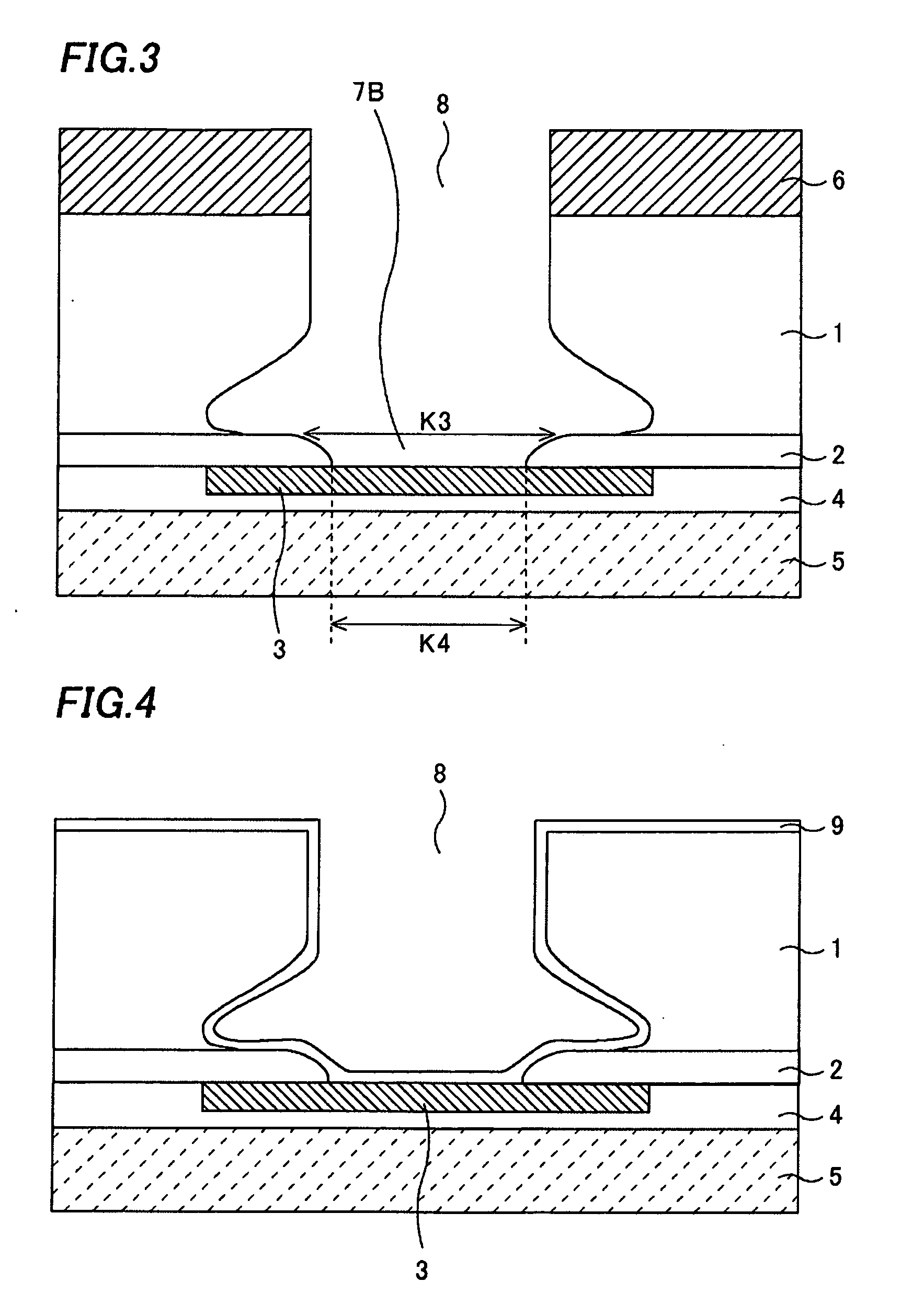
[0052] Next, as shown in FIG. 8, the photoresist layer 6 is formed on the back surface of the semiconductor substrate 1, having an opening corresponding to the pad electrode 3. The semiconductor subrstrate 1 is etched using the photoresist layer 6 as a mask to form the first opening 14 reaching the first insulation layer 2. The etching of the semiconductor substrate 1 is performed so that a diameter Y of the first opening 14 at its bottom becomes larger than a width K5 of the pad electrode 3. The diameter Y of the first opening 14 at its bottom is a diameter thereof on the front surface side of the semiconductor substrate 1 at a boundary of the semiconductor substrate 1 and the first insulation layer 2. It is noted that a numeral K6 in FIG. 8 shows a diameter of the first opening 14 in a portion close to the back surface of the semiconductor substrate 1, and a numeral K7 shows a diameter thereof in a portion laterally widened close to the front surface of the semiconductor substrate...


PUM


Abstract

A semiconductor device with improved reliability and its manufacturing method is offered. The semiconductor device of this invention includes a pad electrode formed on a semiconductor substrate through a first insulation layer, and a via hole formed in the semiconductor substrate and extending from a back surface of the semiconductor substrate to the pad electrode, wherein the via hole includes a first opening of which a diameter in a portion close to the pad electrode is larger than a diameter in a portion close to the back surface of the semiconductor substrate, and a second opening formed in the first insulation layer and continuing from the first opening, of which a diameter in a portion close to the pad electrode is smaller than a diameter in a portion close to the front surface of the semiconductor substrate.

Description

CROSS-REFERENCE OF THE INVENTION [0001] This invention is based on Japanese Patent Application No. 2005-066533, the content of which is incorporated herein by reference in its entirety.BACKGROUND OF THE INVENTION [0002] 1. Field of the Invention [0003] This invention relates to a semiconductor device and its manufacturing method specifically to a technology to form a via hole exposing a pad electrode formed on a semiconductor substrate from a back surface of the semiconductor substrate. [0004] 2. Description of the Related Art [0005] A CSP (Chip Size Package) has received attention in recent years as a three-dimensional mounting technology as well as a new packaging technology. The CSP is a small package having about the same outside dimensions as those of a semiconductor die packaged in it. [0006] A BGA (Ball Grid Array) type semiconductor device has been known as a type of CSP. A plurality of ball-shaped conductive terminals made of a metal such as solder is arrayed in a grid patt...

Claims


Application Information

Patent Timeline
Patent Type & Authority Applications(United States)
IPC IPC(8): H01L23/48H01L21/4763
CPCH01L21/76898H01L23/3114H01L23/481H01L24/11H01L24/12H01L2224/13099H01L2924/01005H01L2924/01013H01L2924/01022H01L2924/01029H01L2924/01033H01L2924/01073H01L2924/01074H01L2924/01078H01L2924/01079H01L2924/01082H01L2924/04941H01L2924/04953H01L2924/01006H01L2924/014H01L24/03H01L24/05H01L24/13H01L2224/0231H01L2224/02372H01L2224/02379H01L2224/05001H01L2224/05008H01L2224/05024H01L2224/05124H01L2224/05147H01L2224/05166H01L2224/05181H01L2224/05184H01L2224/05186H01L2224/05548H01L2224/05569H01L2224/05624H01L2224/05644H01L2224/05647H01L2224/05655H01L2924/12042H01L2924/15788H01L2924/351H01L2924/00H01L2924/00014H01L2924/013H01L22/00H01L23/12
Inventor KAMEYAMA, KOJIROSUZUKI, AKIRAOKAYAMA, YOSHIOUMEMOTO, MITSUO
Owner SEMICON COMPONENTS IND LLC
Why Eureka
Try Eureka