Semiconductor laser

A technology of lasers and semiconductors, applied in semiconductor lasers, structural details of semiconductor lasers, lasers, etc., can solve problems such as poor far-field quality, unsatisfactory small divergence angles, etc., achieve small far-field divergence angles, and reduce catastrophic optical damage risk, the effect of low packaging cost

Active Publication Date: 2019-05-17
HUAZHONG UNIV OF SCI & TECH
View PDF7 Cites 8 Cited by
  • Summary
  • Abstract
  • Description
  • Claims
  • Application Information

AI Technical Summary

Problems solved by technology

[0008] Aiming at the defects of the prior art, the purpose of the present invention is to solve the existing problems such as larger threshold cu...

Method used


Image

  • Semiconductor laser
  • Semiconductor laser
  • Semiconductor laser

Examples


Embodiment 1

[0051] Embodiment 1, the first semiconductor laser with a small divergence angle based on the present invention.

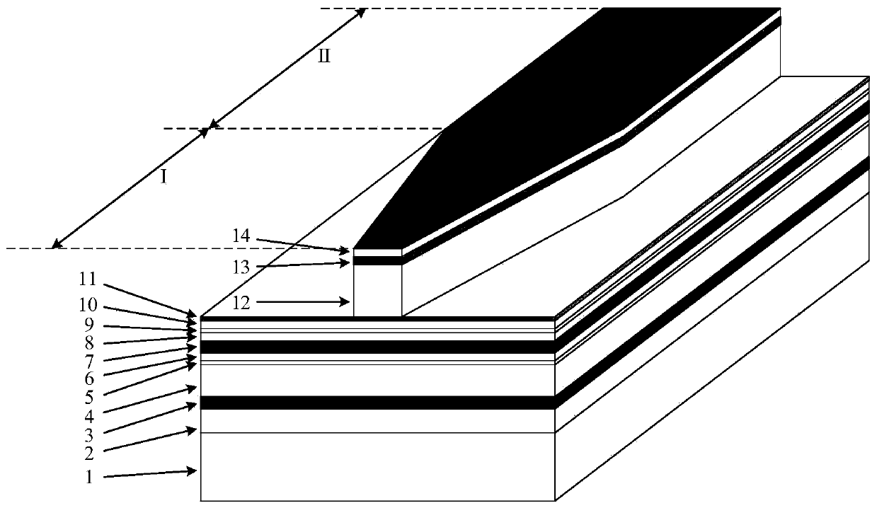
[0052] The working wavelength of the semiconductor laser in this example is 1310nm, and its three-dimensional structure diagram is attached figure 1 , From the substrate layer to the top cover layer are: substrate layer 1, buffer layer 2, lower waveguide core layer 3, lower spacer layer 4, lower barrier layer 5, lower confinement layer 6, active layer 7, upper confinement layer 8. The upper barrier layer 9, the upper spacer layer 10, the corrosion stop layer 11, the upper cladding layer 12, the secondary covering layer 13, and the top covering layer 14. The materials, doping types and thicknesses of each layer are shown in Table 1:

[0053] Table 1 The material, doping type and thickness of each layer in Example 1

[0054]

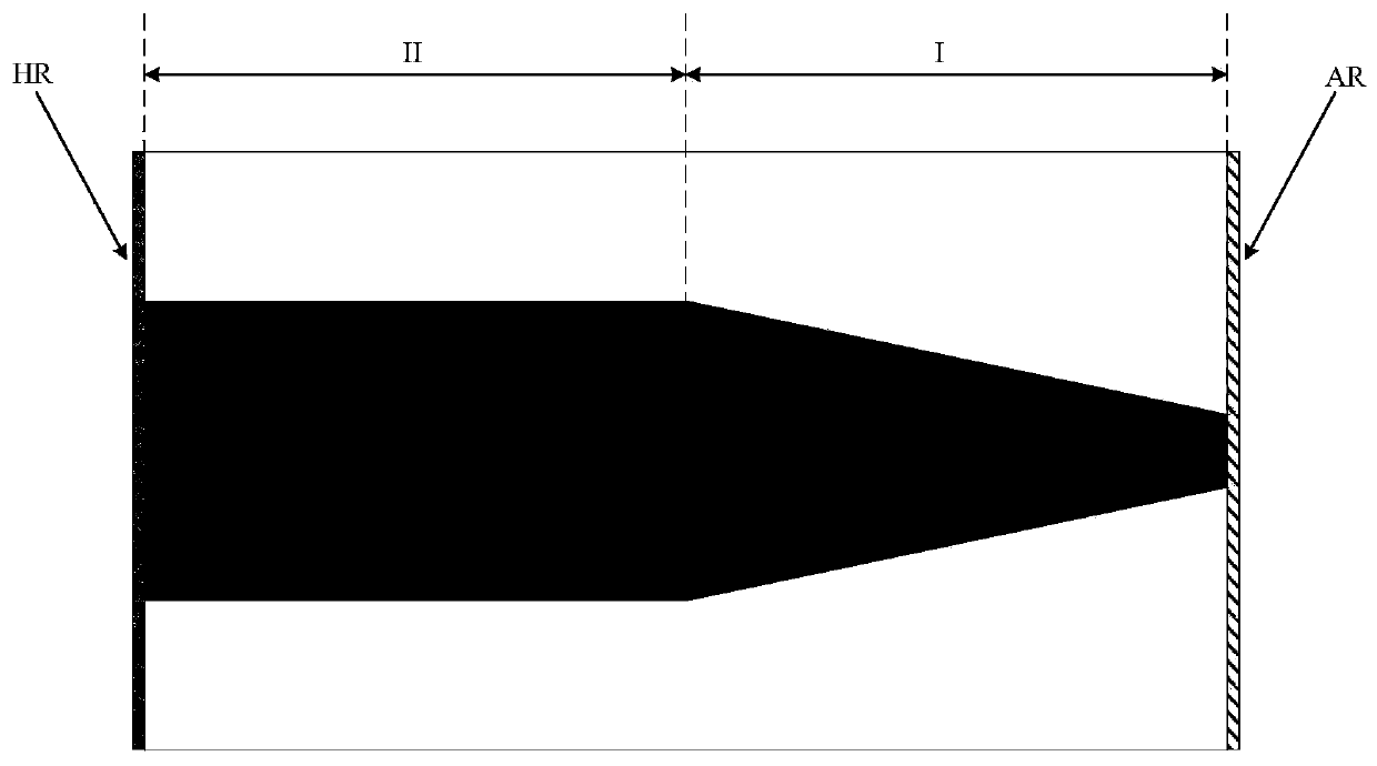
[0055] Wherein, layer 12, layer 13 and layer 14 constitute the ridge of the device by etching, and the bottom of layer 1 and the top of layer 14 are...

Embodiment 2

[0058] Embodiment 2, a second semiconductor laser with a small divergence angle based on the present invention.

[0059] The working wavelength of the semiconductor laser in this example is also 1310nm, and the three-dimensional structure diagram is attached figure 1 , From the substrate layer to the top cover layer are: substrate layer 1, buffer layer 2, lower waveguide core layer 3, lower spacer layer 4, lower barrier layer 5, lower confinement layer 6, active layer 7, upper confinement layer 8. The upper barrier layer 9, the upper spacer layer 10, the corrosion stop layer 11, the upper cladding layer 12, the secondary covering layer 13, and the top covering layer 14. The materials, doping types and thicknesses of each layer are shown in Table 2:

[0060] Table 2 Example 2 Material, doping type and thickness of each layer

[0061] Dielectric layer

material

Doping type

Thickness (nm)

Remarks

Underlayer 1

InP

Type N

---

Buffer layer 2

InP

Type N

300

Lower waveguide co...


PUM


Abstract

The invention discloses a semiconductor laser. The semiconductor laser comprises a lower-part flat plate waveguide and an upper-part ridge waveguide along a growth direction of an epitaxial layer anda ridge width unchanged region at a back side and a ride width narrowing region at a front side along an optical transmission direction, at the ridge width unchanged region, the ridge width of the upper-part ridge waveguide is maintained unchanged, at the ride width narrowing region, the ridge width of the upper-part ridge waveguide is gradually narrowed, the ridge width of a wide ridge end of theride width narrowing region is equal to the ridge width of the ridge width unchanged region, the ridge width of the ridge end of the ride width narrowing region is smaller than the ridge width of thewide ridge end, a narrow ride end is an optical output end, at the ridge width narrowing region, the equivalent refractive index of the upper-part ridge waveguide is gradually reduced with the ridgewidth gradually narrowed until the narrow ridge end approaches the equivalent refractive index of the lower-part flat plate waveguide, the longitudinal size and the transverse size of a base mode of the narrow ridge both are increased, so that the longitudinal scattering angle and the transverse scattering angle of output light both are reduced. The scattering angle of the output light of the semiconductor laser provided by the invention is smaller than the scattering angle of a conventional ridge waveguide-structure semiconductor laser.

Description

Technical field [0001] The present invention relates to the technical field of semiconductor lasers, and more specifically, to a semiconductor laser. Background technique [0002] In the coming era of the Internet of Everything, the demand for communication between people, people and things, and things is increasing rapidly, making optical communication systems play an increasingly important role in the modern information society. All kinds of life, services and industrial applications derived from the developed communication infrastructure are related to the country's technological advancement, the improvement of national strength and people's more convenient life. And the key basic components in the optical communication system, such as the transmitter and receiver, their reliable, high-quality performance determines whether the optical communication system can operate stably, orderly, and long-term effectively with low energy consumption. [0003] In the optical communication s...

Claims


Application Information

Patent Timeline
IPC IPC(8): H01S5/02H01S5/022H01S5/026H01S5/028H01S5/10H01S5/22H01S5/30H01S5/343B82Y20/00
Inventor 李洵兰明文
Owner HUAZHONG UNIV OF SCI & TECH
Why Eureka
Try Eureka