[0011] In a specific embodiment, an alignment mark is a reference area on component that an external probe can use it to monitor the accuracy of component placement on a target platform. The alignment mark incorporated on component can be a conduction path connecting the surface areas from top to bottom on component as a direct alignment mark, or it can be a different conduction path connecting two surface areas at the bottom of component as an indirect alignment mark. Besides being a conduction path within the component, the alignment mark can also be a simple surface marking on component, depending upon the probing method used. The structure of an alignment mark can be a simple geometric structure or a set of geometric structures.
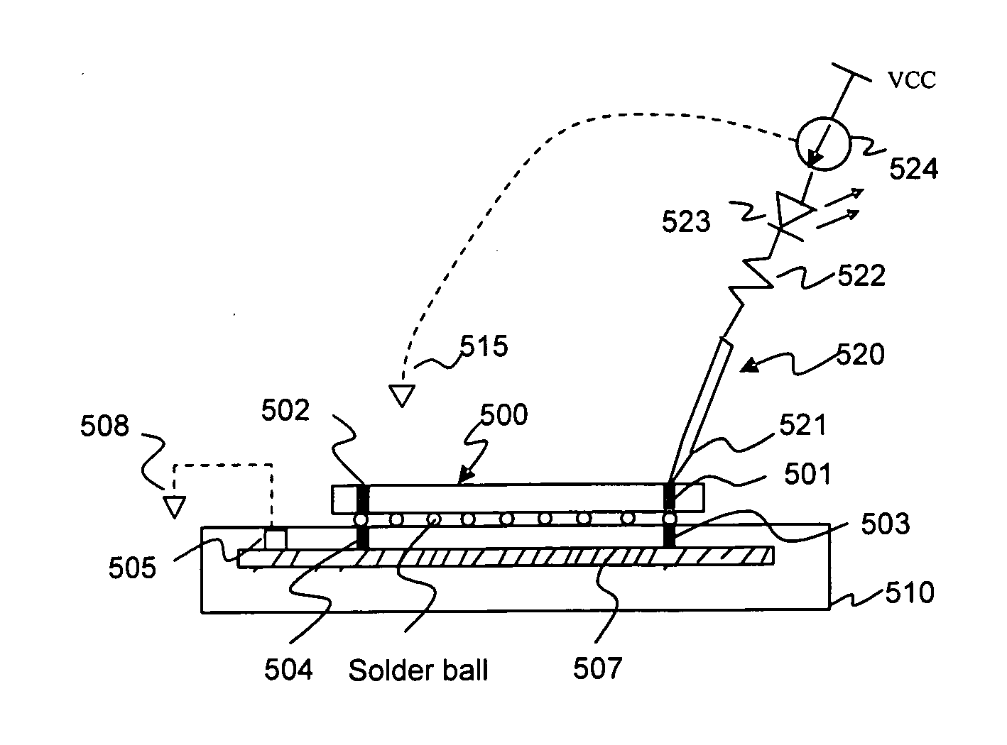
[0013] In preferred embodiments, the present invention provides probe solutions for improving the accuracy in component placement. The probe can be a single-sensor probe or can be an array of sensors. A single-sensor probe can detect the accuracy of component placement and the status of component
contact condition on target platform. A probe composing of an array of sensors to become a multiple-sensor probe can adjust the deviation of displaced component by aligning the one or more alignment marks on component to the probe position that has been aligned to a reference mark. A
multiple sensor probe can detect the deviation of component and feedback the information to the placement equipment to fix the position deviation. While a single alignment mark can fix the component
displacement error, two alignment marks can fix the placement orientation error. The probe can be a resistance probe, a
capacitance probe, an optical probe, or a combination of them. The resistance probe is for on / off measurement, the
capacitance probe is for measuring the relative area overlapping between sensor surface and target reference, and the optical probe is for measuring the reflection from a target reference. The resistance probe is a contact probe. The
capacitance probe and optical probe is a non-contact probe. The range of active sensors on the multiple-sensor probe can be determined automatically by sensing the size of target reference mark.
[0016] Since the
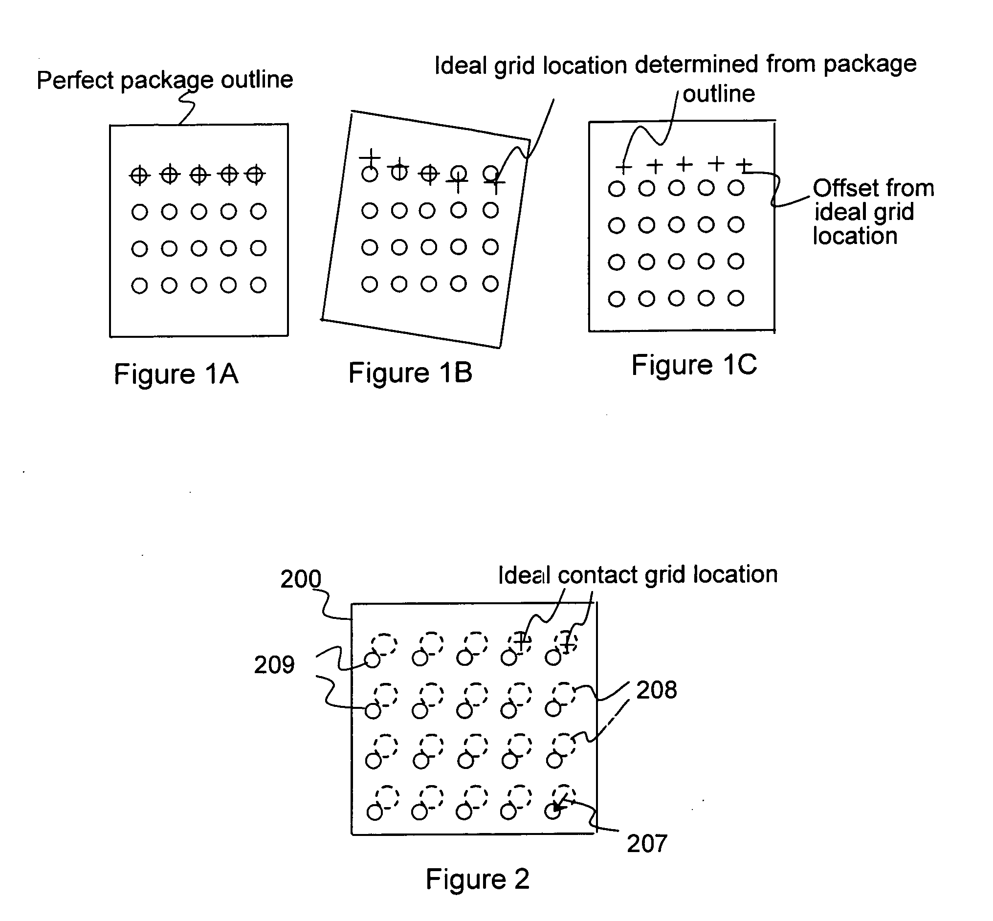
spatial relationship of alignment marks to the associated contact array can be accurately controlled in the device fabrication or component packaging process, a fixed
spatial relationship between the alignment mark and the contact array on device or
package can be ensured. This allows a
package with minor obliquity in physical outline (an oblique
package) or a bare die not perfectly centered-
cut along the scribing line between adjacent dies (off-center-
cut die) can still be used for assembly. This is because in assembly the component placement can then rely on the position of alignment marks, rather than counting on the geometrical tolerance of the package outline. In a specific embodiment, the present invention provides a method for mounting a physically out of specification device or package on a prospective
contact region on PCB or target platform. The physically out of specification devices used to causing misalignment problem in assembly could no longer be rejected. A larger tolerance in the
die cutting of device or in the molding of component package means a higher component yield.
[0017] Many benefits can be achieved by way of the present invention over conventional techniques. The present technique provides an easy to use process that relies upon the conventional technology. In some embodiments, the method provides a mean to improve yields, reduce
rework, and enhance placement accuracy. Additionally, the method provides a process that is compatible with the conventional process technology without substantial modifications to the conventional equipment and processes. The present invention is especially useful for the devices with ultra-fine contact pitch and contact count exceeding hundreds or even a thousand.
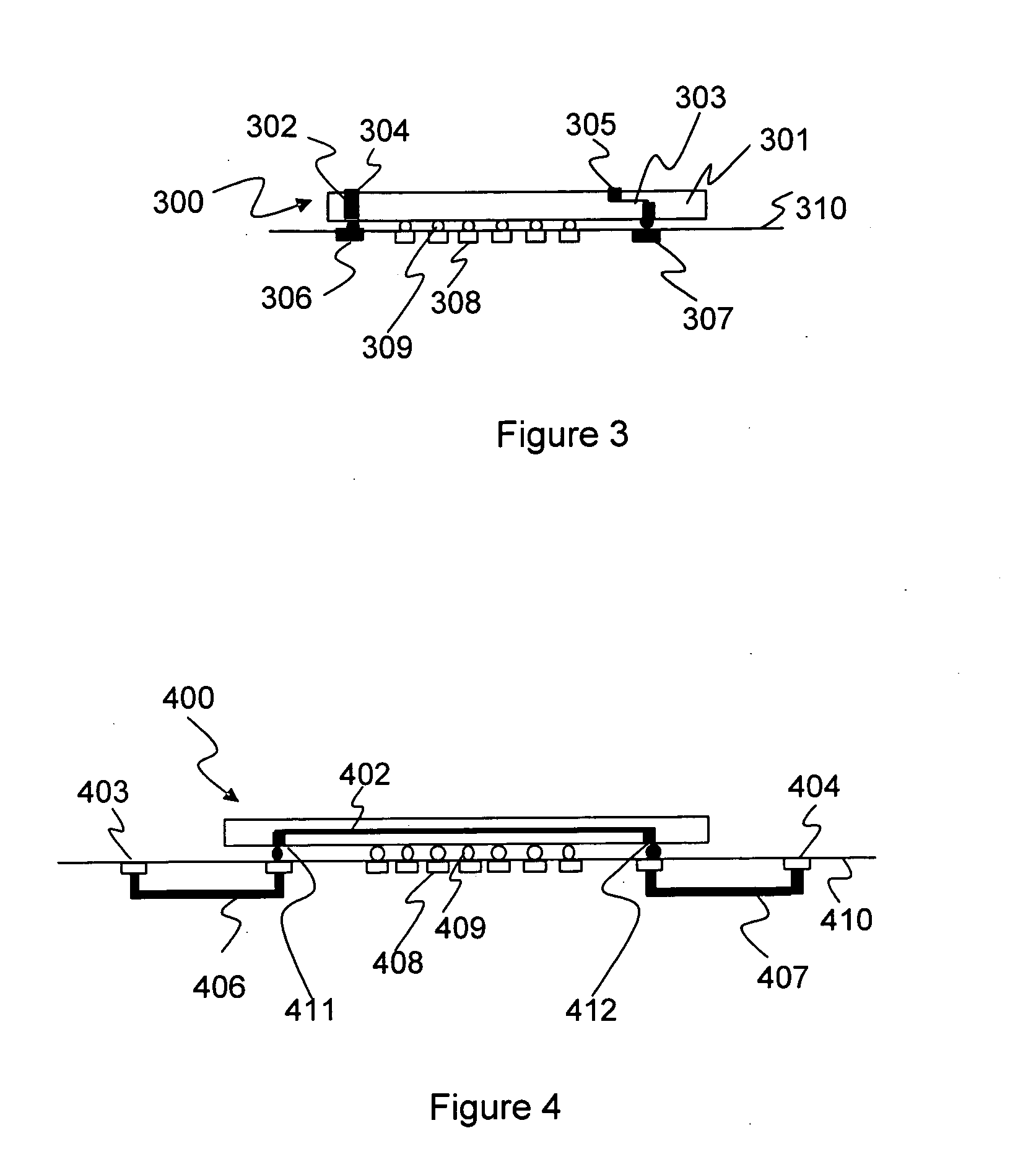
[0018] Moreover, the invention provides a method for monitoring the placement of devices packaged with anisotropic conductive
elastomer (ACE) as interconnect interface. It enables the assembly of non-solder-ball based packaged devices onto target platform or PCB effectively and precisely and thereon for a variety of applications. The anisotropic conductive
elastomer contains a sea of tiny conducting
metal tubes embedded in elastic insulating
silicone membrane that conducts current only in certain direction. It has been used as interconnect in
high density and high pin count test sockets to offer excellent contact,
repeatability, and
high frequency characteristics in IC device test. It is feasible to be as the interface interconnect for devices and packages. A device or component laminated with ACE can be directly mounted onto a target substrate. A clamp shell can be used to hold the devices together without the need of
soldering the devices on target substrate if an accurate placement technology is achievable. The alignment technique can make the assembly of ACE laminated devices on
electronics system feasible.

