Solid-state imaging device, manufacturing method of solid-state imaging device, and camera employing same
a manufacturing method and imaging device technology, applied in the field of solid-state imaging devices, can solve the problems of color separation function, wavelength sensitivity, resolution, wavelength sensitivity, color unevenness, etc., and achieve the effect of reducing the uneven and controlling the thickness of the insulation layer more favorably
- Summary
- Abstract
- Description
- Claims
- Application Information
AI Technical Summary
Benefits of technology
Problems solved by technology
Method used
Image

Examples
first embodiment
[1] First Embodiment
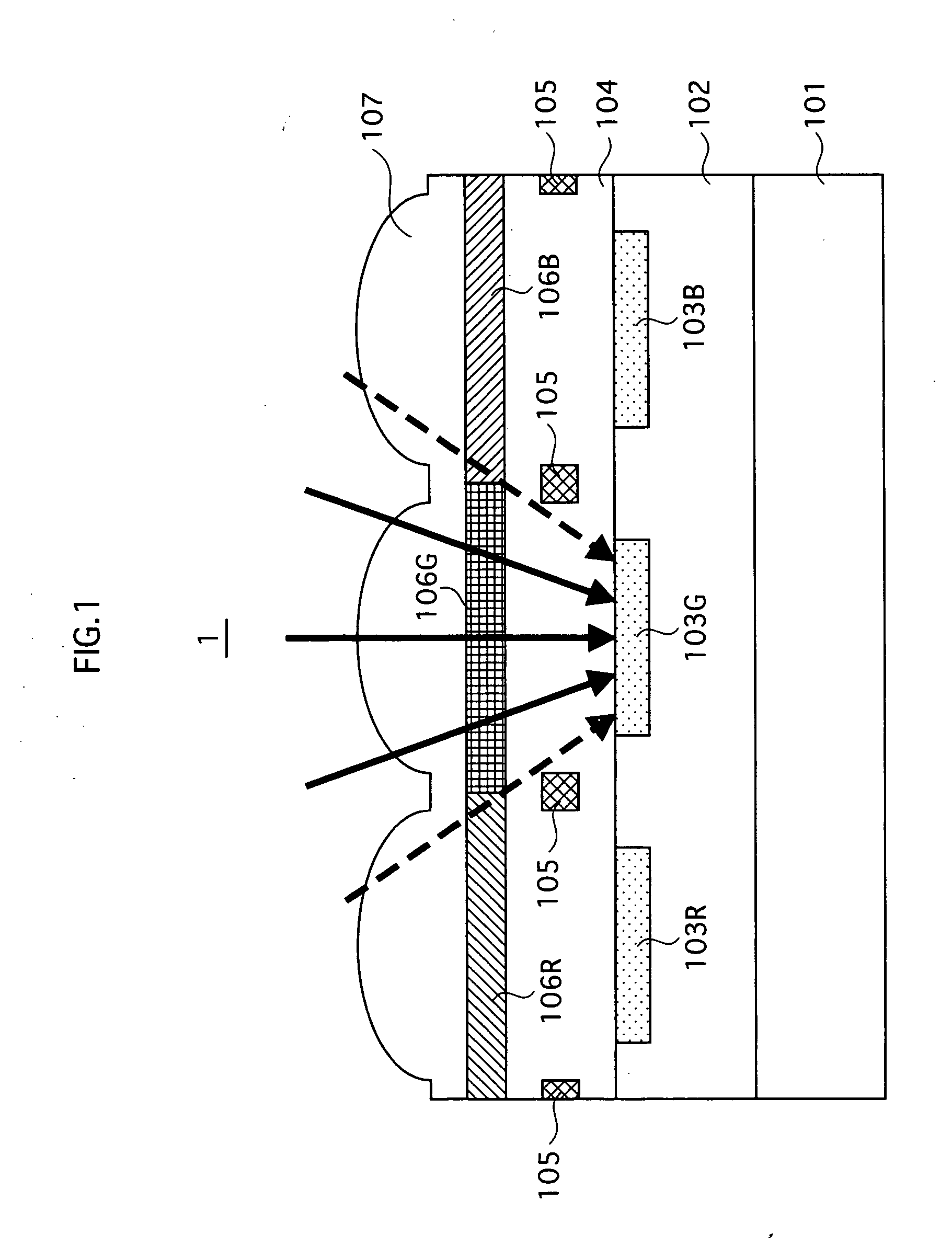
[0077] A solid-state imaging device relating to a first embodiment has substantially the same cross-sectional construction as a conventional solid-state imaging device (see FIG. 1), except for the construction of the color filter.
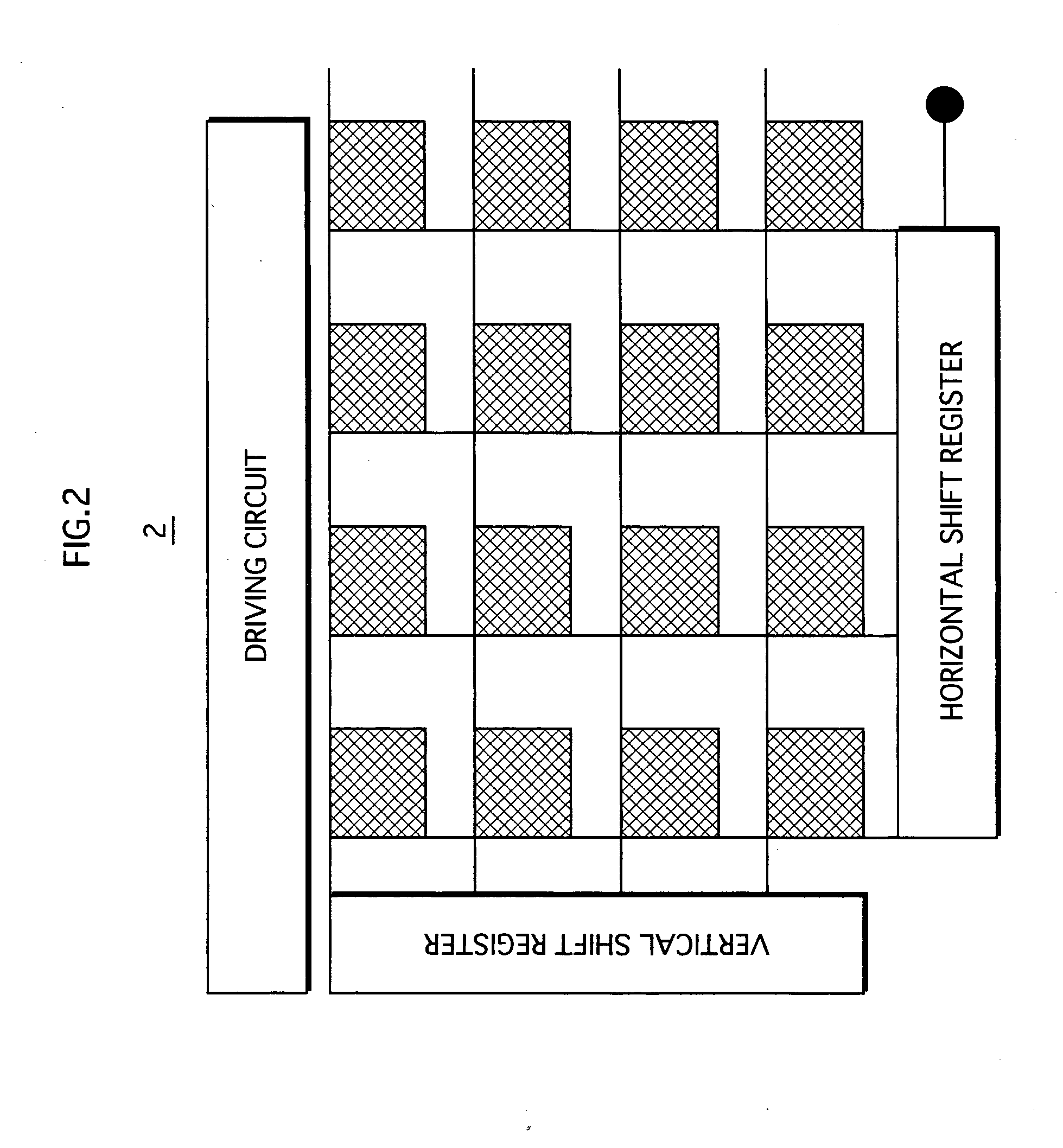
[0078]FIG. 2 is a plan view illustrating the construction of the solid-state imaging device relating to the first embodiment. As shown in FIG. 2, unit pixels (shaded parts), which are light-receiving units, are arranged two-dimensionally in a solid-state imaging device 2 relating to the first embodiment. A vertical shift register selects a row, and a horizontal shift register selects a signal in a pixel in the selected row. In this way, a color signal corresponding to each pixel is output through an output amplifier (not shown in FIG. 2). A driving circuit causes the vertical shift register, horizontal shift register, and output amplifier to operate.
[0079] According to the first embodiment, a color filter is formed by a dielectric mult...
second embodiment
[2] Second Embodiment
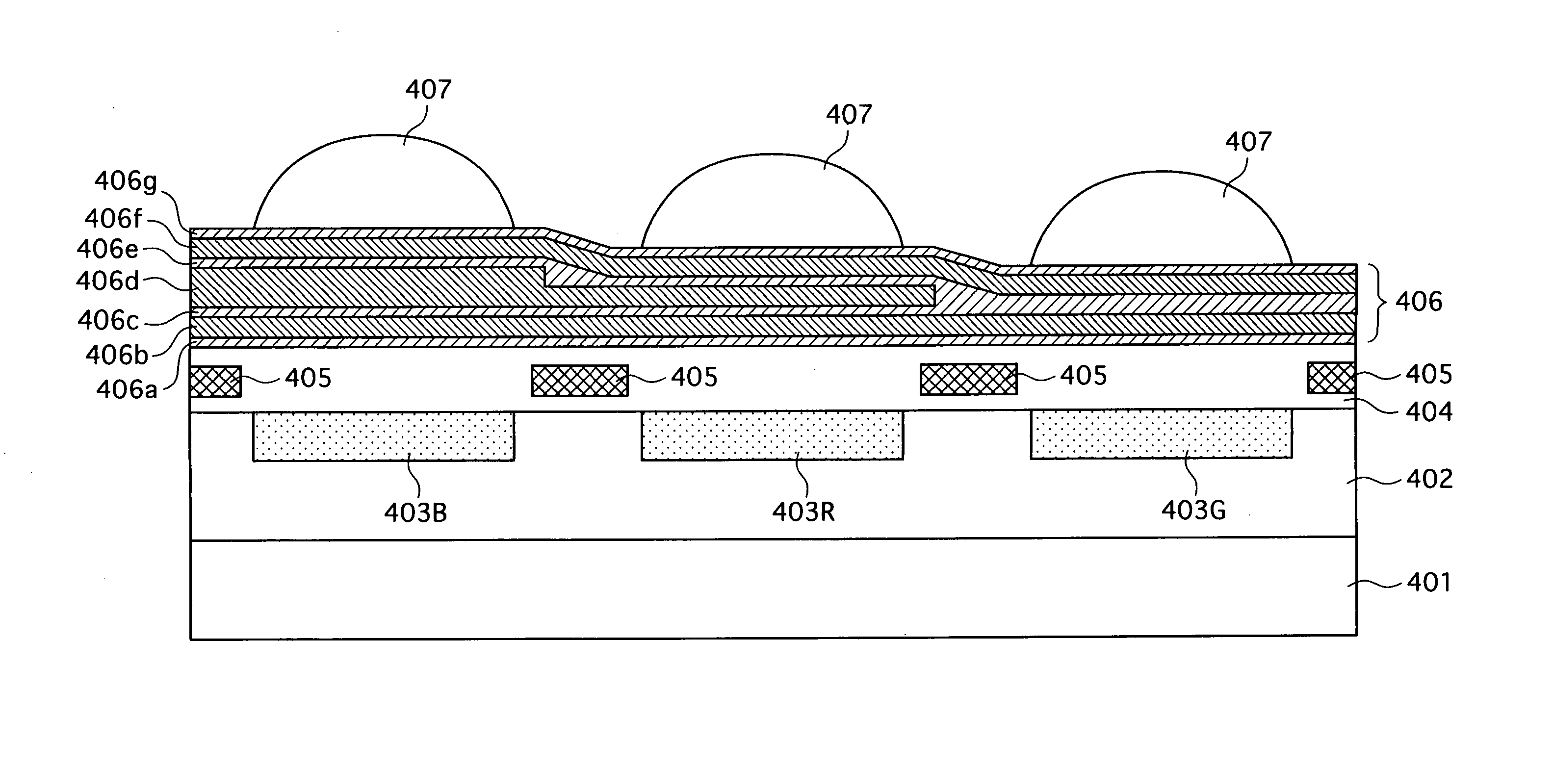
[0082] The following describes a solid-state imaging device relating to a second embodiment of the present invention. The solid-state imaging device relating to the second embodiment has substantially the same construction as the solid-state imaging device relating to the first embodiment, except for the construction of the dielectric multilayer film.
[0083]FIG. 3 is a cross-sectional view illustrating the construction of the solid-state imaging device relating to the second embodiment. As shown in FIG. 3, a solid-state imaging device 4 includes an N-type semiconductor substrate 401, a P-type semiconductor layer 402, light-receiving elements 403R, 403G, and 403B, an insulation layer 404, light-blocking films 405, a color filter 406, and micro lenses 407.
[0084] The solid-state imaging device 4 is structured in such a manner that the P-type semiconductor layer 402, light-receiving elements 403R, 403G, and 403B, insulation layer 404 that can transmit light, light-...
third embodiment
[3] Third Embodiment
[0095] The following describes a solid-state imaging device relating to a third embodiment of the present invention. The solid-state imaging device relating to the third embodiment has the same construction as the solid-state imaging device relating to the second embodiment, except for the manufacturing method of the color filter. The following explains the third embodiment with focus on the manufacturing method of the color filter.
[0096]FIG. 5 illustrates the manufacturing process of the color filter relating to the third embodiment. FIG. 5 does not show the light-blocking films and the like, similarly to FIG. 4.
[0097] To start with, as shown in FIG. 5A, a TiO2 layer 606a, an SiO2 layer 606b, and a TiO2 layer 606c are formed in this order on an insulation layer 604, to form a λ / 4 multilayer structure. Furthermore, a resist 60 having a thickness of 2.5 μm is formed in the red and green regions, on the TiO2 layer 606c, similarly to the second embodiment.
[0098] ...
PUM
 Abstract
Description
Claims
Application Information
 - Generate Ideas
- Intellectual Property
- Life Sciences
- Materials
- Tech Scout
- Unparalleled Data Quality
- Higher Quality Content
- 60% Fewer Hallucinations
Browse by: Latest US Patents, China's latest patents, Technical Efficacy Thesaurus, Application Domain, Technology Topic, Popular Technical Reports.
© 2025 PatSnap. All rights reserved.Legal|Privacy policy|Modern Slavery Act Transparency Statement|Sitemap|About US| Contact US: help@patsnap.com