Method for manufacturing printed circuit board using Ag-Pd alloy nanoparticles

a technology of ag-pd alloy nanoparticles and printed circuit boards, which is applied in the direction of conductive layers on insulating supports, inks, packaging, etc., can solve the problems of deteriorating conductivity, inability to use easy and convenient metal wiring on pcb, and oxidation, etc., to achieve excellent conductivity and anti-migration, competitive price, and excellent

Inactive Publication Date: 2006-09-21
SAMSUNG ELECTRO MECHANICS CO LTD
View PDF13 Cites 62 Cited by
  • Summary
  • Abstract
  • Description
  • Claims
  • Application Information

AI Technical Summary

Benefits of technology

[0012] Also, the present invention provides a method for manufacturing printed circuit board (PCB), having wiring which exhibits competitive price and excellent, conductivity and anti-migration.
[0013] Also, the present invention provides a PCB having wiring formed into fine circuit pattern, which may exhibit competitive price and excellent conductivity and anti-migration, and may not cause disconnection or shorts due to the metal ion migration even at a desired wiring width and spacing.

Problems solved by technology

However, it has some drawbacks: i) the curing temperature is too high; and ii) it requires excess use of anhydrous solvent which is very expensive and risky so that it is not possible to use easy and convenient metal wiring on the PCB.
Moreover, it may deteriorate conductivity because of loose contact between particles.
However, it is very susceptible to oxidation with increases of the surface area of Cu as particle size is getting smaller closer to nano-size and as a result, it forms a silicon dioxide film on the surface by reacting with oxygen in air.
It is difficult to completely avoid the oxidation on the surface although various methods have been tried to prevent the Cu oxidation.
However, Au is very costly so that it causes increase of the manufacturing unit cost.
As a result, it causes disconnection or short between circuits or wirings, and may further damage products.
When high humidity or high temperature condition is eliminated after the migration happened, the migrated state is remained, so that it makes difficult to have confidence of the product.

Method used


Image

  • Method for manufacturing printed circuit board using Ag-Pd alloy nanoparticles
  • Method for manufacturing printed circuit board using Ag-Pd alloy nanoparticles
  • Method for manufacturing printed circuit board using Ag-Pd alloy nanoparticles

Examples


embodiments

[0036] Hereinafter, the present invention will be described in more detail by way of the following embodiments, which are not intended to limit the scope of the present invention.

examples 1 to 5

Preparation of Ag—Pd Alloy Nanopraticle Dispersed Conductive Ink

[0038] 2 Kinds precursors of Palladium acetate and silver acetate precursor were dissolved in 50 Ml of 0.1M sodium dodecyl sulfate (SDS) aqueous solution to have a concentration of 4.5×10⁻⁴ mol. The solution was heated slowly in an oil bath and reacted at 130° C. for 9 hours to obtain an ink dispersed with Ag—Pd alloy nanoparticle size of 1 to 50 nm. Inks with various Pd weight % based on the Ag—Pd alloy were prepared: 5 weight % (example 1); 10 weight % (example 2); 20 weight % (example 3); 30 weight % (example 4); and 40 weight % (example 5),

examples 6 to 10

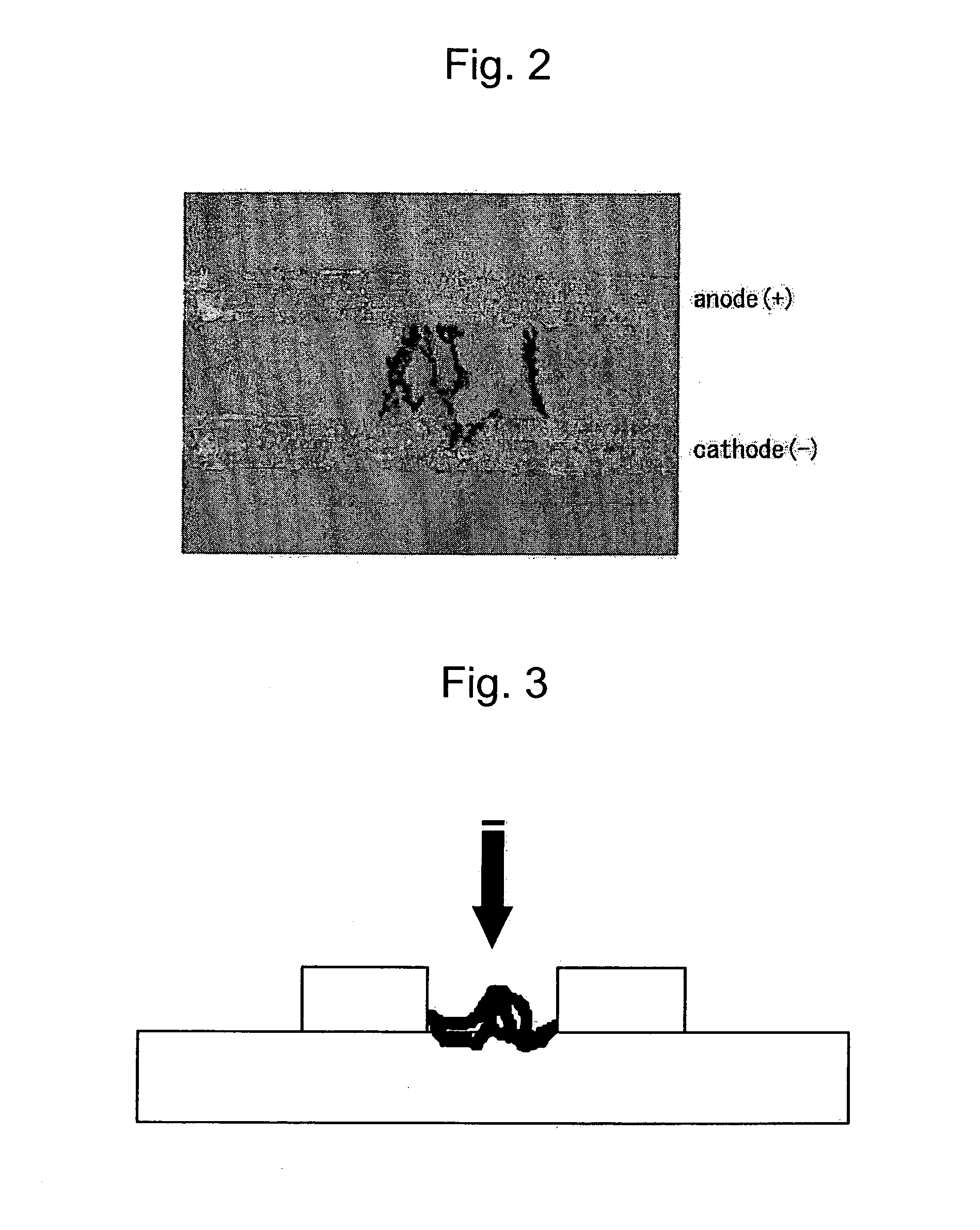
[0040] The conductive ink including Ag—Pd alloy nanoparticles manufactured in examples 1 to 5 was sprayed with L / S 100 microns on a substrate using an ink-jet printer and cured at 250° C. to form wiring. The conductivity of the substrate was measured. 2.5V voltage for 60 seconds to the substrate was applied under the condition of humidity 85%, temperature 85° C. Changes in insulation resistance was observed and the time maintaining the initial insulation resistance (the time forming dendrite) without any changes was detected which was summarized in Table 1 with the result of Comparative example 2. When Pd weight % in the Ag—Pd alloy is 30 weight %, the change in the insulation resistance was illustrated in FIG. 6.

TABLE 1Composition(Ag weight % / ConductivityTime for DendriteCategoryPd weight %)(μΩ· cm)formation(hr)ComparativeAg 1003.2360example. 2Example 695 / 5 5.8560Example 790 / 109.0182.5Example 880 / 2015.8995Example 970 / 3025.74120Example 1060 / 4048.3—

[0041] Referring to Table 1, when...


PUM

PropertyMeasurementUnit
diameteraaaaaaaaaa
diameteraaaaaaaaaa
diameteraaaaaaaaaa

Abstract

The PCB manufactured by spraying conductive ink dispersed with Ag—Pd alloy nanoparticles and curing to form wiring according to the present invention provides reduced migration of Ag ions. Further, the present invention provides a method for manufacturing PCB which exhibits competitive price, and excellent conductivity and anti-migration. As one aspect of the present invention, a conductive ink comprising Ag—Pd alloy nanoparticles, wherein the Ag—Pd alloy nanoparticles includes Pd in the range of from 5 weight % to 40 weight %.

Description

CROSS-REFERENCE TO RELATED APPLICATIONS [0001] This application claims the benefit of Korean Patent Application No. 2005-0022606, filed on Mar. 18, 2005, with the Korea Intellectual Property Office, herein incorporated by reference in its entirety. BACKGROUND OF THE INVENTION [0002] 1. Field of the Invention [0003] The present invention relates to a method for manufacturing a printed circuit board (PCB) by forming a circuit pattern with conductive inks by inkjet printing method. [0004] 2. Description of the Related Art [0005] The metal wiring technology of the printed circuit board (PCB) has been developed in order of etching, screen printing and ink-jet printing technology. Among these, the screen printing technology, which comprises performing screen printing using metal paste and curing, has been known and still widely used. However, it has some drawbacks: i) the curing temperature is too high; and ii) it requires excess use of anhydrous solvent which is very expensive and risky ...

Claims


Application Information

Patent Timeline
Patent Type & Authority Applications(United States)
IPC IPC(8): H01B1/12B22F9/24C09D11/00C09D11/322C09D11/52C22C5/06H01B1/22H01B5/14H01B13/00H05K1/09H05K3/10
CPCC09D11/30H01B1/02H01B1/16H05K1/097H05K3/125A45D40/20A45D40/24A45D2040/201
Inventor CHO, HYE-JINJUN, BYUNG-HO
Owner SAMSUNG ELECTRO MECHANICS CO LTD
Why Eureka
Try Eureka