

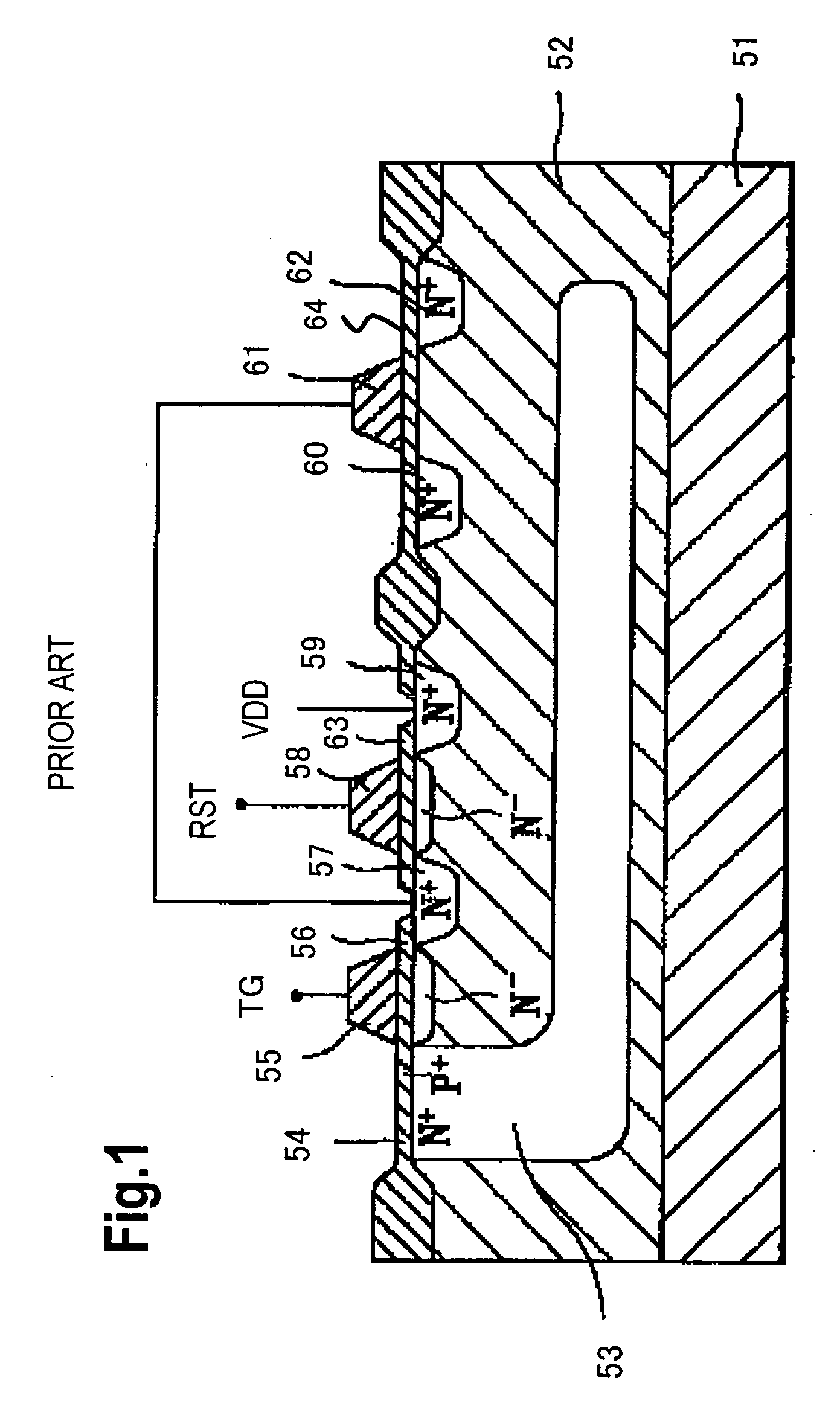
Image sensor with embedded photodiode region and fabrication method thereof
a technology of image sensor and photodiode region, which is applied in the direction of color television, television system, radio control device, etc., can solve the problem of uniform shape of the photodiode region, suppress the addition of noise to the detection signal, and increase the aperture ratio of the pixel in the image sensor. , the effect of increasing the light sensitivity
- Summary
- Abstract
- Description
- Claims
- Application Information
AI Technical Summary
Benefits of technology
Problems solved by technology
Method used
Image

Examples
first embodiment
[0057] First Embodiment
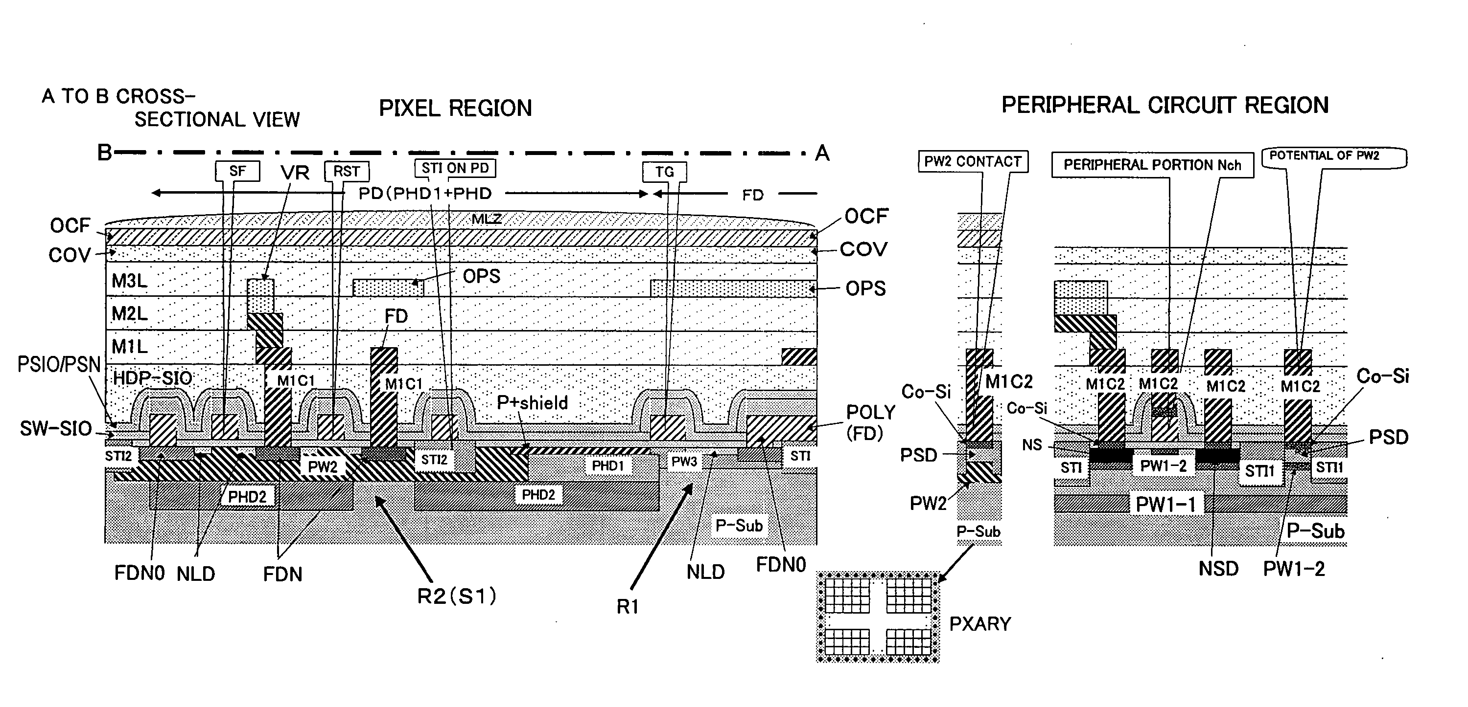
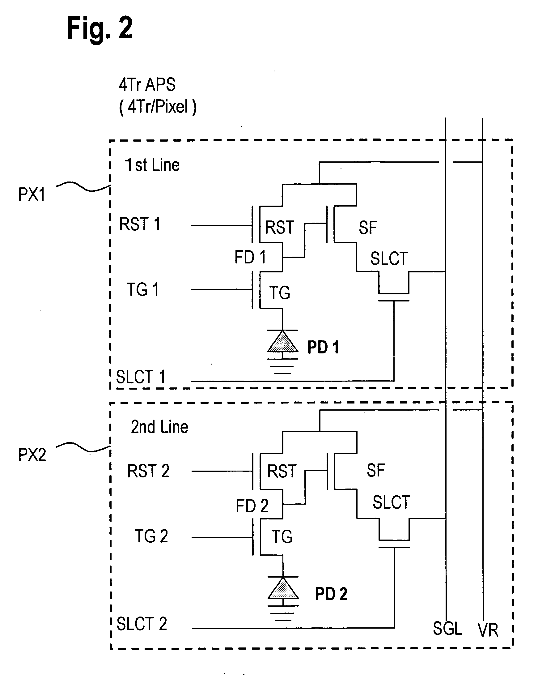
[0058]FIG. 5 is a layout diagram of pixels of the first embodiment. The first embodiment corresponds with the four-transistor-type APS in FIG. 2. FIG. 5 shows a layout with two pixels PX1 and PX2 at the top and bottom respectively. Each of the pixels PX1 and PX2 are isolated by an isolation trench structure STI consisting of a shallow trench isolation (STI), for example, and each pixel is provided with a floating diffusion region FD, a transfer gate transistor TG, a reset transistor RST, a source follower transistor SF, and a select transistor SL (abbreviated as ‘SL’ in the layout). Each transistor comprises a gate electrode TGg, RSTg, SFg, and SLg, the source and drain regions are shown with a bold frame and the in-pixel isolation trench structure is shown as ‘STIp’. Further, the source of the transfer gate transistor TG is a photodiode region PD. The drain of the same transistor TG corresponds to the floating diffusion region FD.
[0059] In addition, in the r...
second embodiment
[0060] Second Embodiment
[0061]FIG. 6 is a layout diagram of pixels of the second embodiment. The second embodiment corresponds with the shared four-transistor-type APS in FIG. 4. FIG. 6 also shows a layout with two pixels PX1 and PX2 at the top and bottom respectively. Each of the pixels PX1 and PX2 are isolated by an isolation trench structure STI consisting of a shallow trench isolation, for example. Further, the two pixels PX1 and PX2 share a floating diffusion region FD, a reset transistor RST, a source follower transistor SF, and a select transistor SL and both pixels comprise a transfer gate transistor TG on the sides above and below the shared floating diffusion region FD. Further, the shared floating diffusion region FD is disposed above the boundary between the two pixels PX1 and PX2.
[0062] So too in FIG. 6, each transistor comprises gate electrodes TGg, RSTg, SFg, and SLg. The source and drain regions thereof are shown with a bold frame and the in-pixel isolation trench s...
third embodiment
[0098] Third Embodiment
[0099]FIG. 12 is a layout diagram of pixels of the third embodiment. Like the second embodiment of FIG. 6, the two upper and lower pixels PX1 and PX2 share the floating diffusion region FD and the transistors RST, SF, and SL. The third embodiment differs from the second embodiment in that a photodiode region PD with a diagonal pattern is not formed below the source follower transistor SF, the source follower transistor SF is disposed on the pixel boundary line BNDRY, and the reset transistor RST and select transistor SL are arranged above and below the boundary line. Because the photodiode region PD (PHD2) is not provided below the source follower transistor SF, it is possible to reduce the substrate bias effect by the photodiode region PD to the P-type well region PW2 constituting the channel region of the transistor SF.
[0100] Further, the layout of the transistors TG, RST, SL, and SF has line symmetry with respect to the boundary line BNDRY, the pixel layou...
PUM
 Abstract
Description
Claims
Application Information