Power semiconductor devices and methods of manufacture
What is AI technical title?
AI technical title is built by Patsnap AI team. It summarizes the technical point description of the patent document.
a technology of semiconductor devices and semiconductors, applied in the direction of electric variable regulation, process and machine control, instruments, etc., can solve the problems of improving the voltage performance of transistors while maintaining a low rdson, and achieves improved voltage performance, reduced parasitic capacitance, and high switching speed
Inactive Publication Date: 2006-09-28
SEMICON COMPONENTS IND LLC
View PDF99 Cites 222 Cited by
Summary
Abstract
Description
Claims
Application Information
AI Technical Summary
This helps you quickly interpret patents by identifying the three key elements:
Problems solved by technology
Method used
Benefits of technology
Benefits of technology
[0025] The present invention provides various embodiments for power devices, as well as their methods of manufacture, packaging, and circuitry incorporating the same for a wide variety of power electronic applications. Broadly, one aspect of the invention combines a number of charge balancing techniques and other techniques for reducing parasitic capacitance to arrive at various embodiments for power devices with improved voltage performance, higher switching speed, and lower on-resistance. Another aspect of the invention provides improved termination structures for low, medium and high voltage devices. Improved methods of fabrication for power devices are provided according to other aspects of the invention. Improvements to specific processing steps, such as formation of trenches, formation of dielectriclayers inside trenches, formation of mesa structures, processes for reducing substrate thickness, among others are offered by various embodiments of the invention. According to another aspect of the invention, charge balanced power devices incorporate temperature and current sensing elements such as diodes on the same die. Other aspects of the invention improve equivalent series resistance (ESR), or gate resistance, for power devices, incorporate additional circuitry on the same chip as the power device and provide improvements to the packaging of charge balanced power devices.
Problems solved by technology
For example, in the case of the power MOSFET, because of the proportional relationship between the drain-to-source on-resistance RDSon and the breakdown voltage, improving the voltage performance of the transistor while maintaining a low RDSon poses a challenge.
Method used
Image
Click on the blue label to locate the original text in one second.
Reading with bidirectional positioning of images and text.
Examples
Embodiment Construction
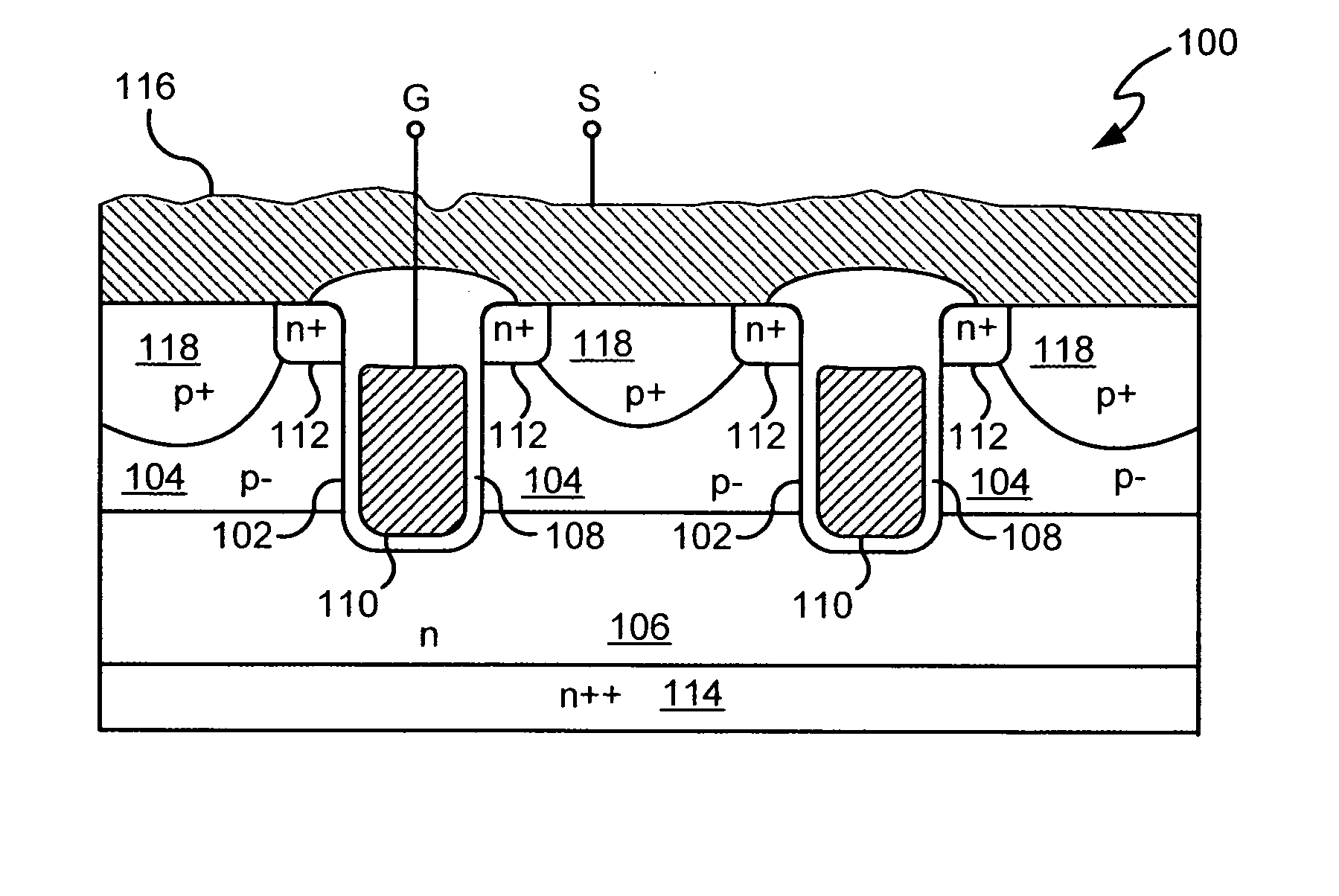
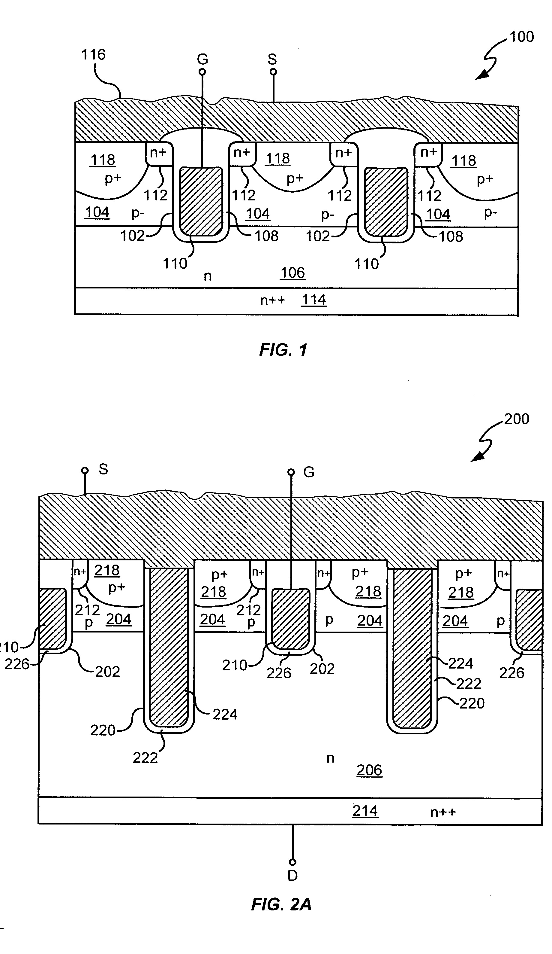
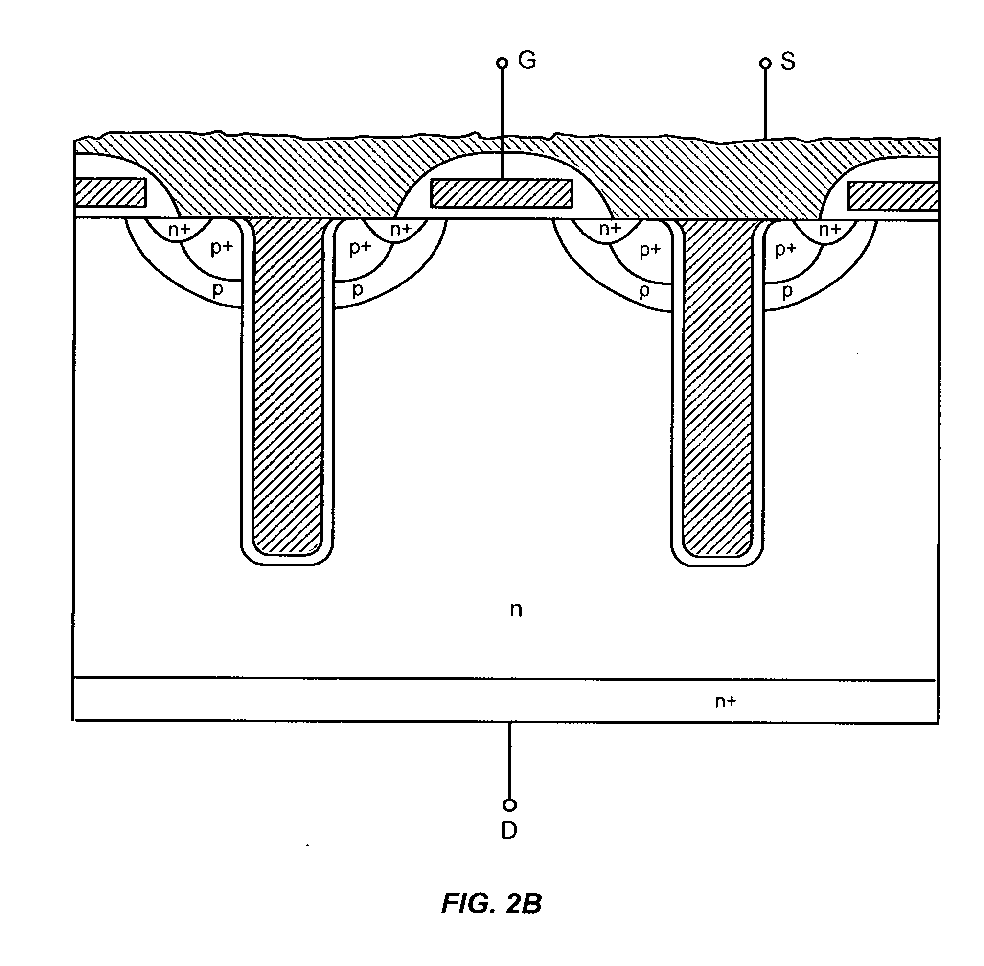
[0108] The power switch can be implemented by any one of power MOSFET, IGBT, various types of thyristors and the like. Many of the novel techniques presented herein are described in the context of the power MOSFET for illustrative purposes. It is to be understood however that the various embodiments of the invention described herein are not limited to the power MOSFET and can apply to many of the other types of power switch technologies, including, for example, IGBTs and other types of bipolar switches and various types of thyristors, as well as diodes. Further, for the purposes of illustration, the various embodiments of the invention are shown to include specific p and n type regions. It is understood by those skilled in the art that the teachings herein are equally applicable to devices in which the conductivities of the various regions are reversed.
[0109] Referring to FIG. 1, there is shown a cross-sectional view of a portion of an exemplary n-type trench power MOSFET 100. As w...
PUM
Abstract
Various embodiments for improved power devices as well as their methods of manufacture, packaging and circuitry incorporating the same for use in a wide variety of power electronic applications are disclosed. One aspect of the invention combines a number of charge balancing techniques and other techniques for reducing parasitic capacitance to arrive at different embodiments for power devices with improved voltage performance, higher switching speed, and lower on-resistance. Another aspect of the invention provides improved termination structures for low, medium and high voltage devices. Improved methods of fabrication for power devices are provided according to other aspects of the invention. Improvements to specific processing steps, such as formation of trenches, formation of dielectriclayers inside trenches, formation of mesa structures and processes for reducing substrate thickness, among others, are presented. According to another aspect of the invention, charge balanced power devices incorporate temperature and current sensing elements such as diodes on the same die. Other aspects of the invention improve equivalent series resistance (ESR) for power devices, incorporate additional circuitry on the same chip as the power device and provide improvements to the packaging of charge balanced power devices.
Description
CROSS-REFERENCES TO RELATED APPLICATIONS [0001] This application is a continuation of the following commonly-assigned U.S. patent application: [0002] Ser. No. 11 / 026,276 (Attorney Docket No. 18865-133-1 / 67260.00), entitled “Power Semiconductor Devices and Methods of Manufacture,” by Ashok et al., filed Dec. 29, 2004; [0003] which claims the benefit of the following provisionally-filed U.S. patent application: [0004] No. 60 / 533,790 (Attorney Docket No. 18865-133 / 17732-67260), entitled “Power Semiconductor Devices and Methods of Manufacture,” by Ashok et al., filed Dec. 30, 2003; [0005] and is a continuation-in-part of the following commonly-assigned U.S. patent applications: [0006] Ser. No. 10 / 640,742 (Attorney Docket No. 90065.000241 / 17732-66550), entitled “Improved MOS Gating Method for Reduced Miller Capacitance and Switching Losses,” by Kocon et al., filed Aug. 14, 2003; [0007] Ser. No. 10 / 442,670 (Attorney Docket No. 18865-131 / 17732-66850), entitled “Structure and Method for For...
Claims
Application Information
Patent Timeline
Application Date:The date an application was filed.
Publication Date:The date a patent or application was officially published.
First Publication Date:The earliest publication date of a patent with the same application number.
Issue Date:Publication date of the patent grant document.
PCT Entry Date:The Entry date of PCT National Phase.
Estimated Expiry Date:The statutory expiry date of a patent right according to the Patent Law, and it is the longest term of protection that the patent right can achieve without the termination of the patent right due to other reasons(Term extension factor has been taken into account ).
Invalid Date:Actual expiry date is based on effective date or publication date of legal transaction data of invalid patent.
Patent Type & AuthorityApplications(United States)
InventorCHALLA, ASHOKELBANHAWY, ALANGREBS, THOMAS E.KRAFT, NATHAN L.PROBST, DEAN E.RIDLEY, RODNEY S.SAPP, STEVEN P.WANG, QIYUN, CHONGMANLEE, J.G.WILSON, PETER H.YEDINAK, JOSEPH A.JUNG, J.Y.JANG, H.C.SANI, BABAK S.STOKES, RICHARDDOLNY, GARY M.MYTYCH, JOHNLOSEE, BECKYSELSLEY, ADAMHERRICK, ROBERTMURPHY, JAMES J.MADSON, GORDON K.MARCHANT, BRUCE D.REXER, CHRISTOPHER L.KOCON, CHRISTOPHER B.WOOLSEY, DEBRA S.

