Memory chip architecture with high speed operation

Active Publication Date: 2006-10-05
SK HYNIX INC
View PDF17 Cites 2 Cited by
  • Summary
  • Abstract
  • Description
  • Claims
  • Application Information

AI Technical Summary

Benefits of technology

[0014] An embodiment of the invention is a semiconductor memory device having a chip architecture for reducing a chip size to thereby increase the number of die per wafer in order to improve a characteristic of mass production.
[0016] An embodiment of the invention is a semiconductor memory device that may allow for fast developing a cutdown product having a substantially identical characteristic and a different cell density by arranging control blocks for performing a data access in order to achieve a simple modification.
[0017] An embodiment of the invention is a semiconductor memory device that may substantially equalize an access timing of each bank in response to inputted command and address by using a transmission control block between each bank and control and address pads.
[0018] In accordance with an aspect of the present invention, there is provided a semiconductor memory device for increasing an integration to improve an operation speed and a power consumption of the semiconductor memory device, including at least one data transmission block including data I / O pads arranged in a major-axis side of the semiconductor memory device; a command and address transmission block including address and command input pads arranged in at least one minor-axis side of the semiconductor memory device; a global line block, arranged in a center of the semiconductor memory device, for transmitting inputted command and address; and at least one bank area, arranged between the global line block and the data transmission block, each bank area containing plural data I / O blocks located in a side of the data transmission block and plural control blocks located in a side of the global line block to thereby minimize paths for transmitting a data, a command and an address for increasing the integration.

Problems solved by technology

However, as above described, the unit block constituted with four banks should include each four of the I / O sense amplifiers I / O-S / As, the write drivers wdrvs, the column decoders Y-decs, the row decoders X-decs and the data access control blocks X,Y_ctrls; thus, current consumption for performing the data access is increased and an operation speed of the conventional graphic DDR SDRAM becomes slow.
Also, because of the I / O sense amplifiers I / O-S / As, the write drivers wdrvs, the column decoders Y-decs, the row decoders X-decs and the data access control blocks X,Y_ctrls, the conventional graphic DDR SDRAM cannot reduce a die size; as a result, a characteristic for mass production is still bad.

Method used


Image

  • Memory chip architecture with high speed operation
  • Memory chip architecture with high speed operation
  • Memory chip architecture with high speed operation

Examples


Embodiment Construction

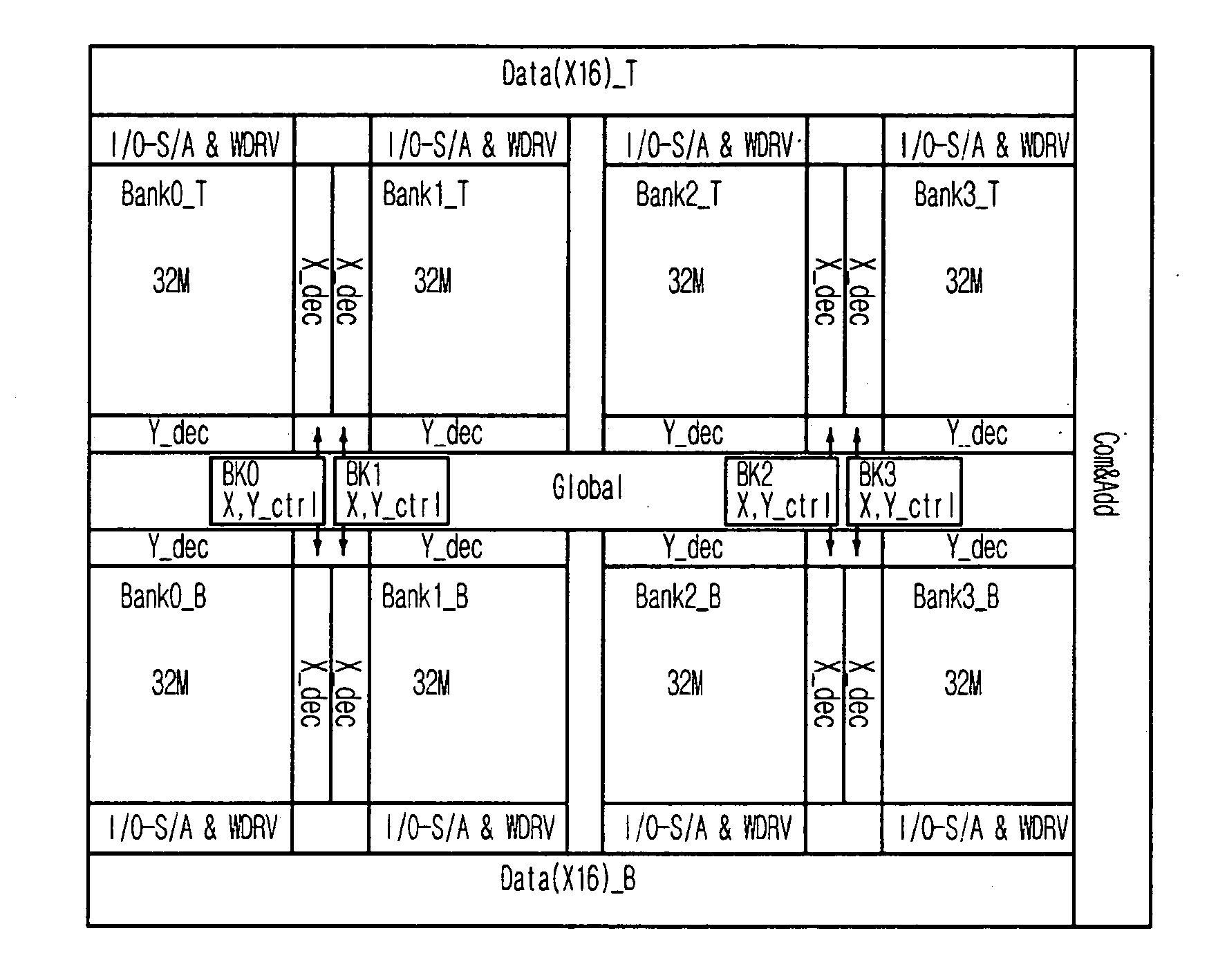
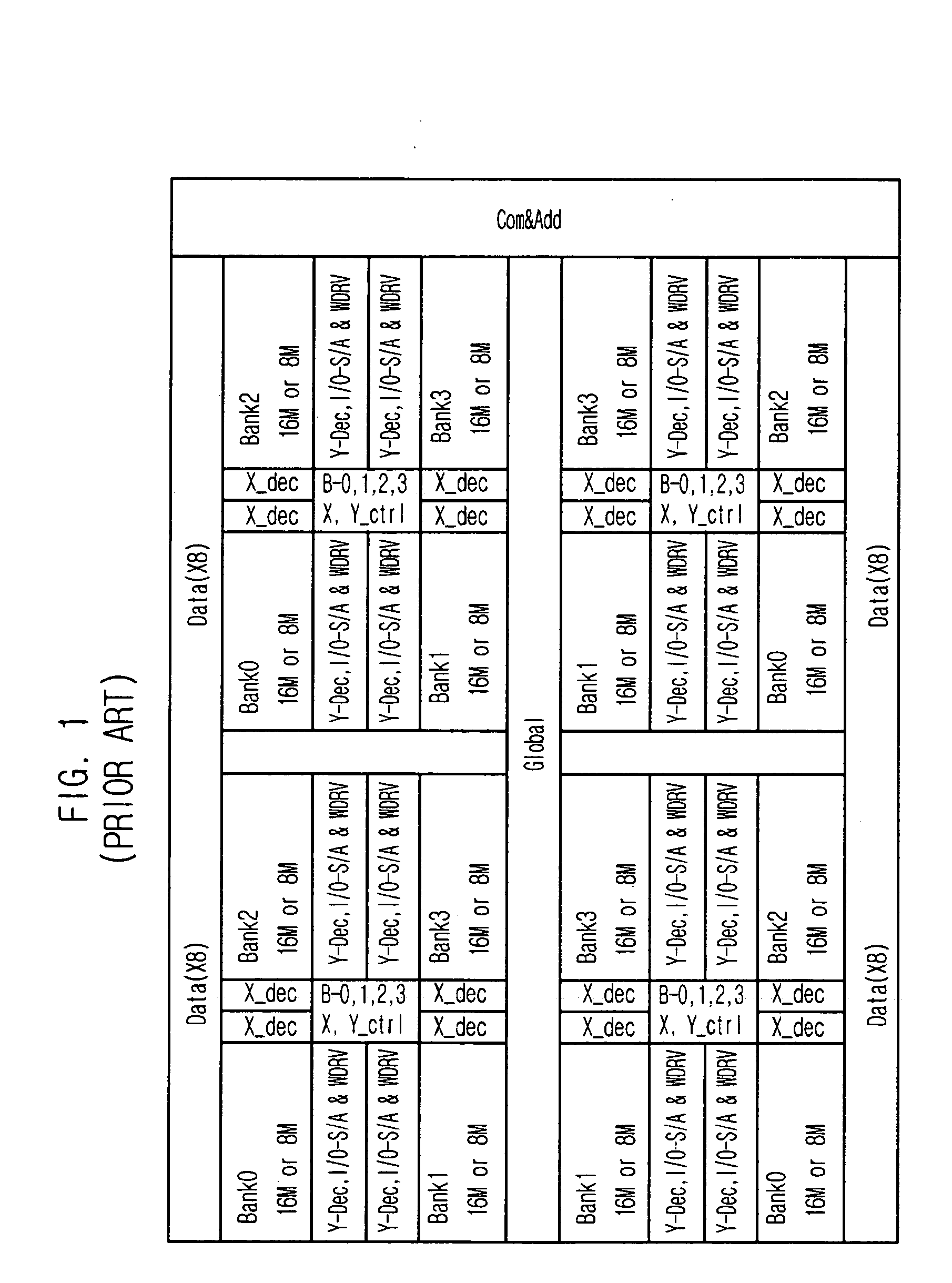
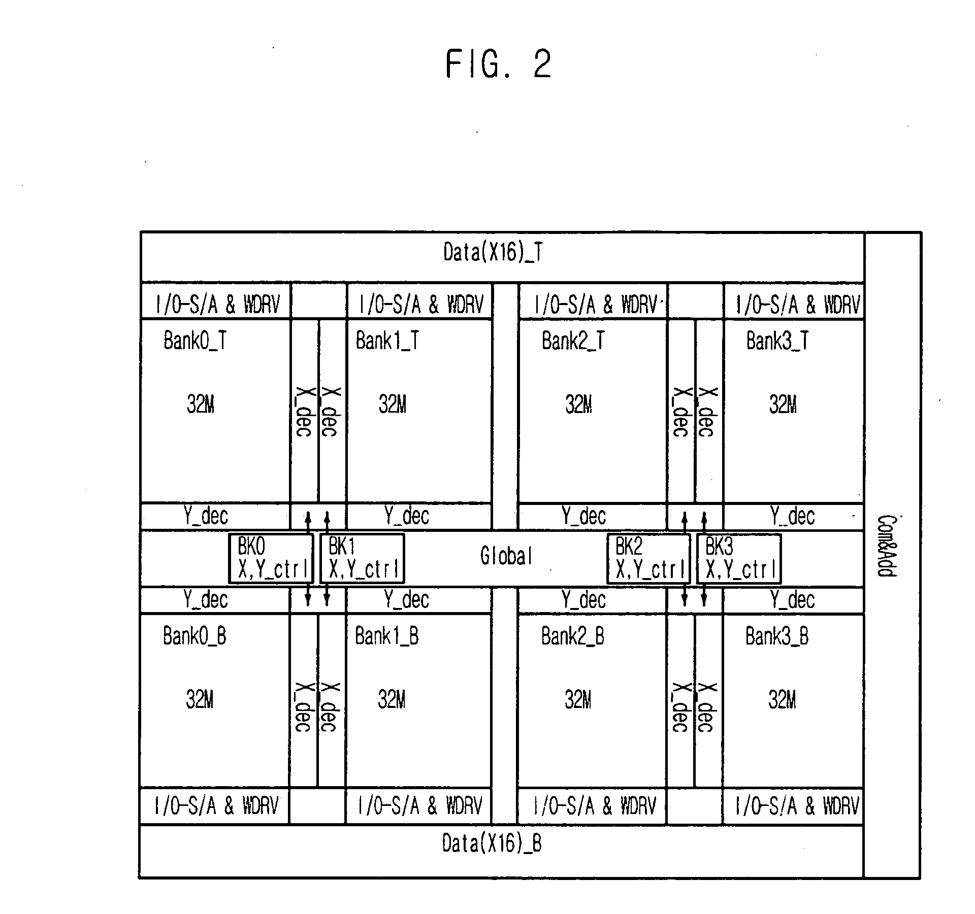
[0028] Hereinafter, a memory device in accordance with specific embodiments of the present invention will be described in detail with reference to the accompanying drawings.

[0029] A semiconductor memory device according to the present invention increases an integration to improve operation speed and power consumption of the semiconductor memory device. The semiconductor memory device includes at least one data transmission block including data I / O pads arranged in a major-axis side of the semiconductor memory device; a command and address transmission block including address and command input pads arranged in at least one minor-axis side of the semiconductor memory device; a global line block, arranged in a center of the semiconductor memory device, for transmitting inputted command and address; and at least one bank area, arranged between the global line block and the data transmission block, each bank area containing plural data I / O blocks located in a side of the data transmissi...


PUM


Abstract

A semiconductor memory device includes at least one data transmission block including data I / O pads arranged in a major-axis side of the semiconductor memory device; a command and address transmission block including address and command input pads arranged in at least one minor-axis side of the semiconductor memory device; a global line block, arranged in a center of the semiconductor memory device, for transmitting inputted command and address; and at least one bank area, arranged between the global line block and the data transmission block, each bank area containing plural data I / O blocks located in a side of the data transmission block and plural control blocks located in a side of the global line block.

Description

FIELD OF INVENTION [0001] An embodiment of the invention relates to a semiconductor memory device; and, more particularly, to a chip architecture of the semiconductor memory device. DESCRIPTION OF RELATED ARTS [0002] Generally, a memory device such as a dynamic random access memory (DRAM) is used in a computer and a communication device. Moreover, there is a need to operate the memory device at higher frequencies; thus, the memory device is fabricated for stable high-speed operation. In addition, for reducing fabrication cost of the memory device, there is a need to minimize a die size of the memory device. [0003] Conventionally, a semiconductor memory device includes a plurality of banks, each for performing a data access independently. Each bank includes a row decoder (X-decoder), a column decoder (Y-decoder), an I / O sense amplifier, a write driver, an address control block, and other functional blocks for supporting the data access. The semiconductor memory device performs the da...

Claims


Application Information

Patent Timeline
IPC IPC(8): G11C8/00
CPCG11C11/4097
Inventor LEE, GEUN-ILJOO, YONG-SUK
Owner SK HYNIX INC
Why Eureka
Try Eureka