Method for manufacturing SIMOX wafer

Inactive Publication Date: 2006-10-12
SUMCO CORP
View PDF35 Cites 8 Cited by
  • Summary
  • Abstract
  • Description
  • Claims
  • Application Information

AI Technical Summary

Benefits of technology

[0018] It is thus an object of the present invention to provide a method for manufacturing a SIMOX wafer which is capable of

Problems solved by technology

However, a number of problems are associated with such high-dose SIMOX wafers, including the generation of numerous threading dislocations and a long time needed for oxygen ion implantation, which raises production costs.
However, the BOX layer in the above low-dose SIMOX wafer has a small thickness, resulting in a decline in the reliability of the BOX layer.
Yet, even with a low-dose SIMOX process that incorporates this ITOX technique, because the oxygen ion dose remains high at 4×10¹⁷ atoms/cm2, ion implantation takes several hours per batch, in addition to which ITOX treatment must also be carried out.
As a result, heat

Method used


Image

  • Method for manufacturing SIMOX wafer
  • Method for manufacturing SIMOX wafer
  • Method for manufacturing SIMOX wafer

Examples


Example

Example 1

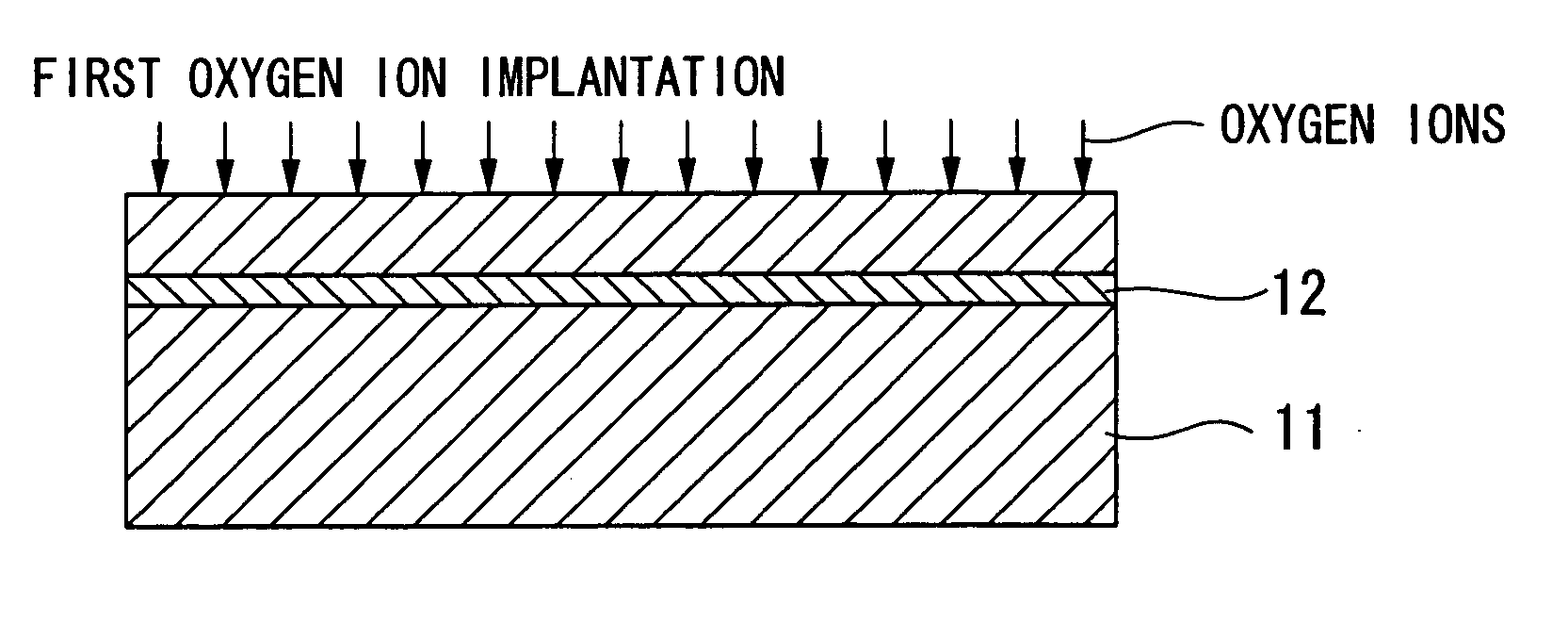
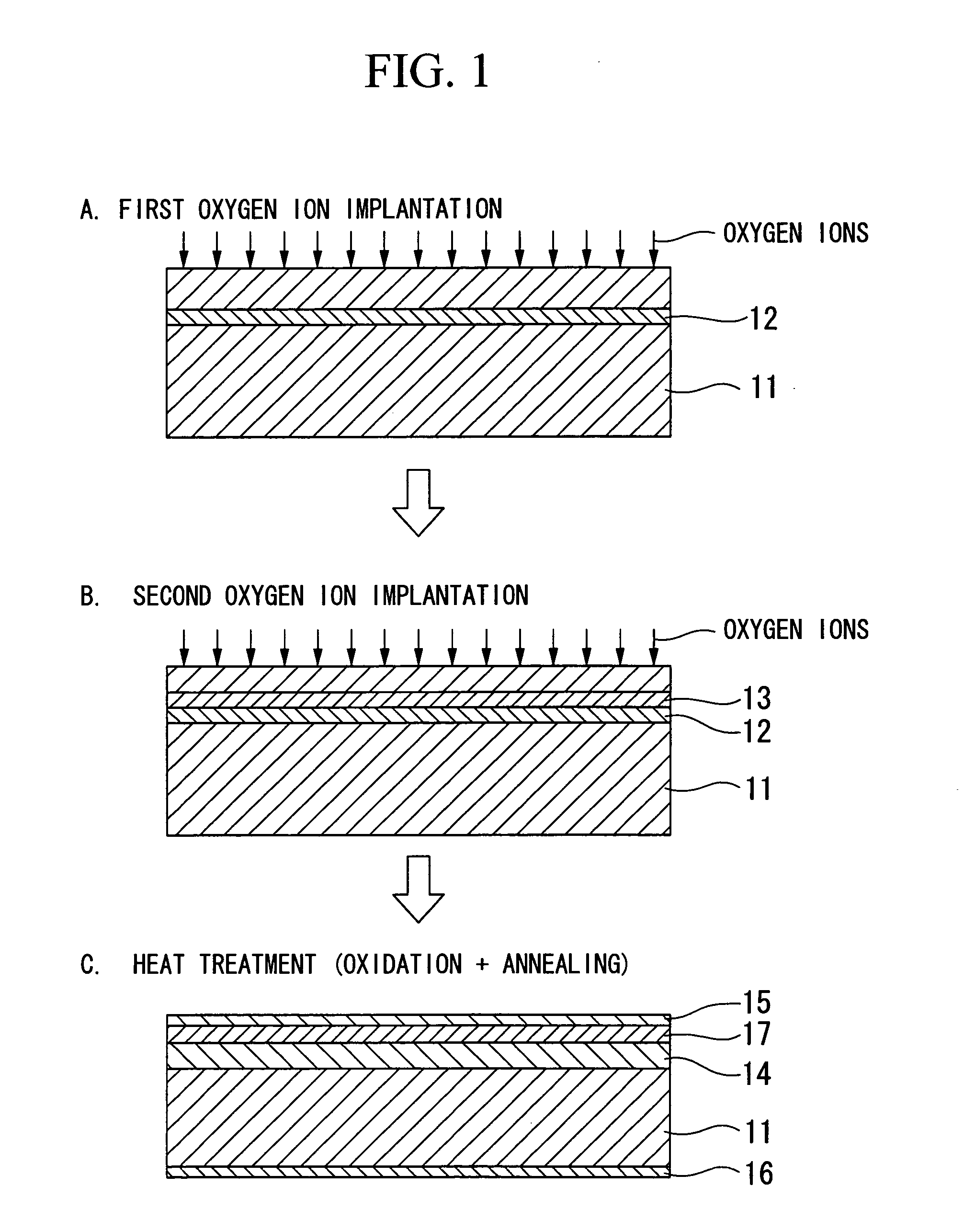
[0050] A silicon wafer 11 was manufactured by the MLD-SIMOX process, as shown in FIG. 1. First, oxygen ion implantation of the wafer 11 was carried out in two steps. In the first oxygen ion implantation step, the wafer 11 was heated in a vacuum to 400° C., and implantation was carried out at an oxygen ion dose of 3×10¹⁷ atoms / cm2. In the second oxygen ion implantation step, which immediately followed the first oxygen ion implantation step, the temperature of the wafer 11 was lowered to room temperature and implantation was carried out at an oxygen ion dose of 2×10¹⁵ atoms / cm2. In this way, the surface of the wafer 11 remained a single crystal and a high oxygen concentration layer 12 and an amorphous layer 13 were formed in the wafer 11.

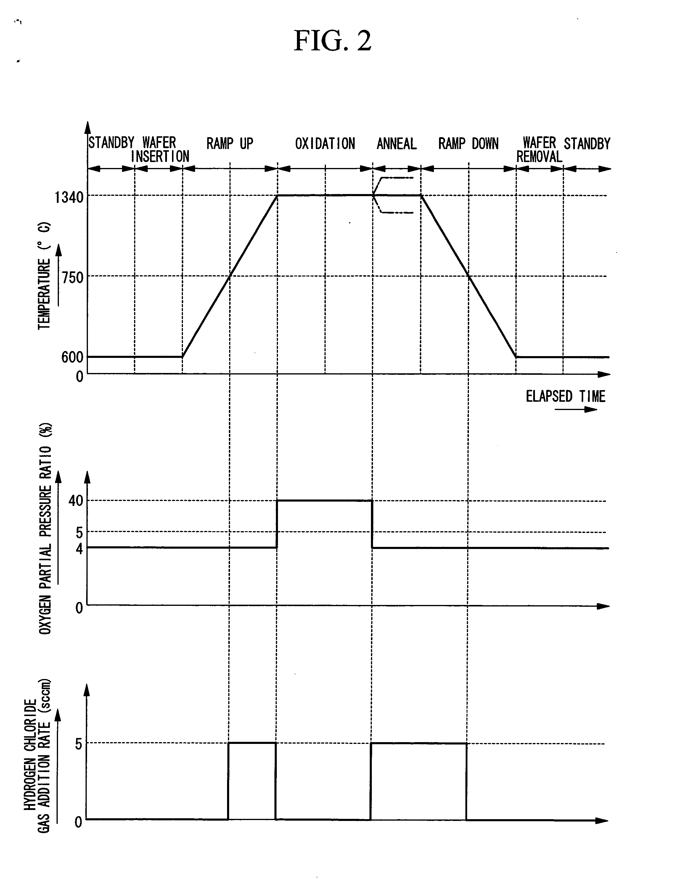
[0051] Next, the wafer 11 was placed in a heat treatment furnace, the temperature was raised to 1340° C. at a ramp rate of 1° C. / min in a ramp-up step, held at 1340° C. for 10 hours in an oxidation treatment step, held at 1340° C. for 5 hou...

Example

Example 2

[0052] In the wafer ramp-down step, treatment was carried out by feeding argon gas containing oxygen in a partial pressure ratio of 4% to the heat treatment furnace at a flow rate of 25 slm, feeding trans-LC along with a carrier gas at a flow rate of 5 sccm, and mixing the two gases. In the wafer ramp-up step and anneal step, treatment was carried out by feeding only argon gas containing oxygen in a partial pressure ratio of 4% to the heat treatment furnace at a flow rate of 25 slm. In the wafer oxidation treatment step, treatment was carried out by feeding only argon gas containing oxygen in a partial pressure ratio of 40% to the heat treatment furnace at a flow rate of 25 slm. Aside from the above, a wafer was manufactured in the same way as in Example 1. This wafer was “Example 2”.

Example

Example 3

[0053] In the wafer ramp-up step, treatment was carried out by feeding argon gas containing oxygen in a partial pressure ratio of 4% to the heat treatment furnace at a flow rate of 25 slm, feeding trans-LC along with a carrier gas at a flow rate of 5 sccm, and mixing the two gases. In the wafer anneal step and ramp-down step, treatment was carried out by feeding only argon gas containing oxygen in a partial pressure ratio of 4% to the heat treatment furnace at a flow rate of 25 slm. In the wafer oxidation treatment step, treatment was carried out by feeding only argon gas containing oxygen in a partial pressure ratio of 40% to the heat treatment furnace at a flow rate of 25 slm. Aside from the above, a wafer was manufactured in the same way as in Example 1. This wafer was “Example 3”.


PUM

PropertyMeasurementUnit
Fractionaaaaaaaaaa
Partial pressureaaaaaaaaaa

Abstract

In the method for manufacturing a SIMOX wafer, oxygen ions are implanted into a silicon wafer, then the silicon wafer is subjected to a prescribed heat treatment so as to form a buried oxide layer in the silicon wafer. The prescribed heat treatment includes: a step of ramping up a temperature of the silicon wafer in a low oxygen partial pressure gas atmosphere having an oxygen partial pressure ratio of less than 5%; either or both of a step of oxidizing the silicon wafer in a high oxygen partial pressure gas atmosphere having an oxygen partial pressure ratio of 5% or more and a step of annealing the silicon wafer in a low oxygen partial pressure gas atmosphere having an oxygen partial pressure ratio of less than 5%; and a step of ramping down the temperature of the silicon wafer in a low oxygen partial pressure gas atmosphere having an oxygen partial pressure ratio of less than 5%. A hydrogen chloride gas is mixed with the low oxygen partial pressure gas having an oxygen partial pressure ratio of less than 5% in at least one step from among the ramp-up step, the anneal step and the ramp-down step.

Description

BACKGROUND OF THE INVENTION [0001] 1. Field of the Invention [0002] The present invention relates to a method for manufacturing a SIMOX (Separation by IMplanted OXygen) wafer. More specifically, the invention relates to a method for manufacturing a SIMOX wafer having reduced metal contamination in a surface and having a buried oxide layer with an excellent dielectric withstanding voltage. [0003] 2. Background Art [0004] The SIMOX process (see Reference Document 1, for example) is familiar as one type of a method for manufacturing a silicon-on-insulator (SOI) wafer. In the SIMOX process, oxygen ions are implanted at an acceleration energy of about 200 keV and a dose of about 2×10¹⁸ atoms / cm2 to form an as-implanted (referring to the state following oxygen ion implantation and before heat treatment) stoichiometric buried oxide (BOX) layer, after which heat treatment is performed to regenerate a crystallinity of the SOI layer and modify the BOX layer. SIMOX wafers manufactured by this ...

Claims


Application Information

Patent Timeline
IPC IPC(8): C23C14/00B05D3/02
CPCC23C8/12C23C8/80H01L21/76243C30B29/06C30B33/005C23C14/48
Inventor AOKI, YOSHIROSUDO, MITSURUNAKAI, TETSUYA
Owner SUMCO CORP
Why Eureka
Try Eureka