Plasma processing apparatus, plasma processing method and wave retardation plate
a processing apparatus and wave retardation plate technology, applied in plasma techniques, coatings, chemical/physical/physico-chemical processes, etc., can solve the problems of difficult to adopt such a structure, the interference of the microwave propagating inside the wave retardation plate, and the inability to use the antenna thereafter. , to achieve the effect of efficient plasma generation, less variation with time, and good reproducibility
- Summary
- Abstract
- Description
- Claims
- Application Information
AI Technical Summary
Benefits of technology
Problems solved by technology
Method used
Image

Examples
first embodiment
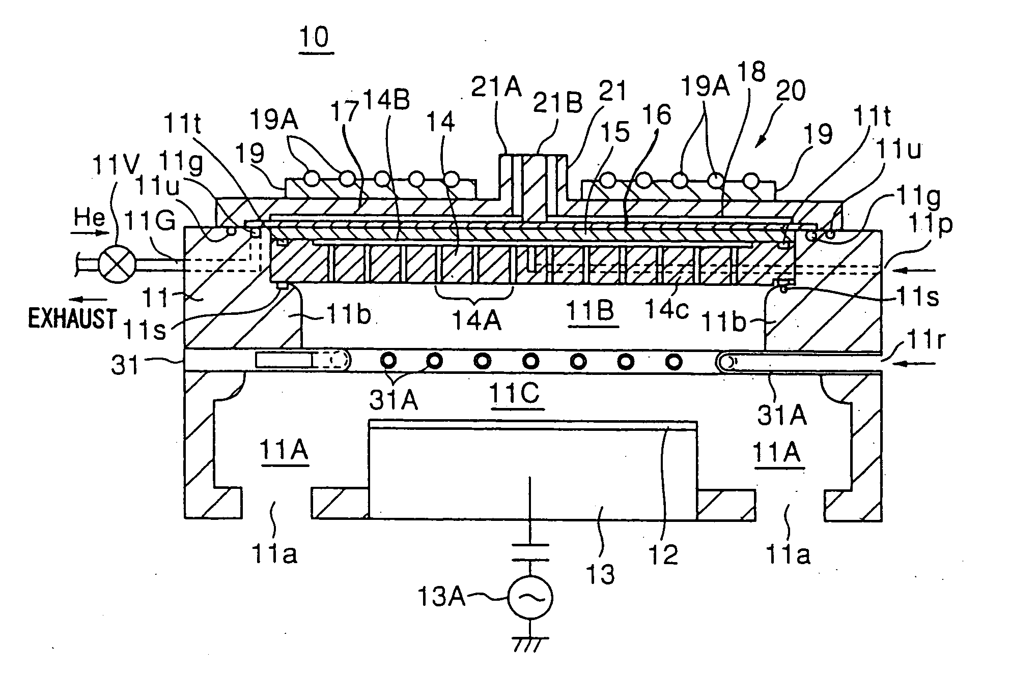
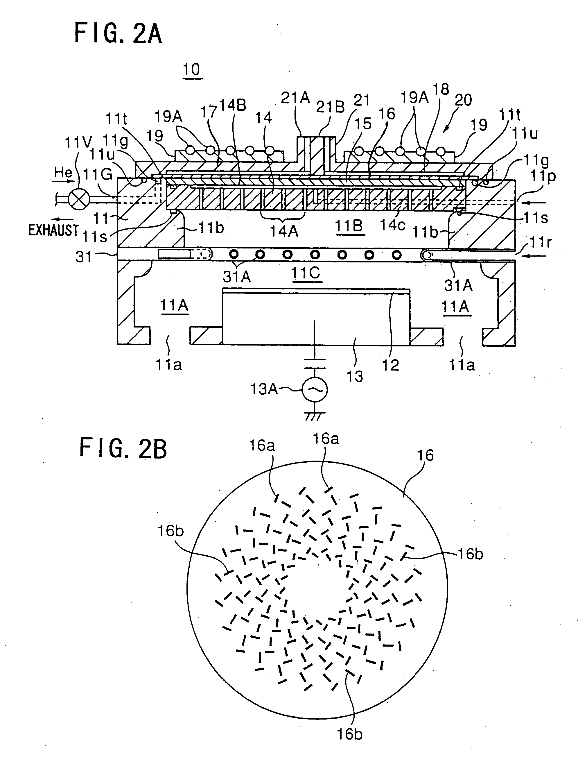
[0065]FIGS. 2A and 2B are diagrams showing the construction of a microwave plasma processing apparatus 10 according to a first embodiment of the present invention.
[0066] Referring to FIG. 2A, the microwave plasma processing apparatus 10 includes a processing vessel 11 and a stage 13 provided in the processing vessel 11 for holding a substrate 12 to be processed by an electrostatic chuck, wherein the stage 13 is preferably formed of AlN or Al2O3 by a hot isostatic pressing (HIP) process. In the processing vessel 11, there are formed two or three evacuation ports 11a in a space 11A surrounding the stage 13 with an equal distance, and hence with an axial symmetry with respect to the substrate 12 on the stage 13. The processing vessel 11 is evacuated to a low pressure via the evacuation port 11a by a gradational lead screw pump to be explained later.
[0067] The processing vessel 11 is preferably formed of an austenite stainless steel containing Al, and there is formed a protective film...
second embodiment
[0090]FIG. 6 shows a composition of a plasma processing apparatus 10B according to a second embodiment of the present invention. In FIG. 6, parts that are explained previously are given the same reference numerals, and descriptions thereof will be omitted.
[0091] With reference to FIG. 6, a microwave antenna 20A is used instead of the microwave antenna 20 of FIG. 2A in the present embodiment. In the microwave antenna 20A, an end portion 21b of a core conductor 21B of a coaxial waveguide 21 is separated from the slot plate 16, and is coupled to a back of the wave retardation plate 18 formed on the slot plate 16. With this composition, a microwave can be efficiently supplied without bringing the core conductor 21B into contact with the slot plate 16. In the above-mentioned microwave antenna 20A, the wave retardation plate 18 is continuously extended on the back of the slot plate 16, and the contact hole for the core conductor is not formed.
[0092]FIGS. 7A-7D are illustrations showing ...
third embodiment
[0100]FIG. 8 is an outline structure diagram of a microwave plasma processing apparatus according to an embodiment of the present invention.
[0101] The microwave plasma processing apparatus 40 shown in FIG. 8 is, for example, a plasma CVD apparatus, which applies-plasma CVD processing to a semiconductor wafer W as a substrate to be processed in a processing vessel 42. The processing vessel 42 is formed of aluminum, for example, and has a hermetic construction so as to be evacuatable. There is provided a placement table 44 for placing the semiconductor wafer W in the processing container 42.
[0102] The bottom of the processing vessel 42 is provided with an exhaust port 42a to which a vacuum pump (not shown) is connected so that the interior of the processing vessel 42 can be maintained in a predetermined low-pressure state.
[0103] The dielectrics plate 46 is airtightly attached to a ceiling part of the processing vessel 42. In the present embodiment, a wave retardation plate 48, whic...
PUM
| Property | Measurement | Unit |
|---|---|---|
| thickness | aaaaa | aaaaa |
| gate length | aaaaa | aaaaa |
| temperature | aaaaa | aaaaa |
Abstract
Description
Claims
Application Information
 - R&D
- Intellectual Property
- Life Sciences
- Materials
- Tech Scout
- Unparalleled Data Quality
- Higher Quality Content
- 60% Fewer Hallucinations
Browse by: Latest US Patents, China's latest patents, Technical Efficacy Thesaurus, Application Domain, Technology Topic, Popular Technical Reports.
© 2025 PatSnap. All rights reserved.Legal|Privacy policy|Modern Slavery Act Transparency Statement|Sitemap|About US| Contact US: help@patsnap.com