
Multi-quantum well optical waveguide with broadband optical gain

a broadband optical gain and optical waveguide technology, applied in the field of optical waveguides, can solve the problems of carrier gap between two quantum well materials cannot be too different, carrier injection efficiency degradation,

Inactive Publication Date: 2006-10-19
CHOA FOW SEN +1
View PDF2 Cites 12 Cited by
  • Summary
  • Abstract
  • Description
  • Claims
  • Application Information

AI Technical Summary

Benefits of technology

[0008] In one embodiment, single transverse-mode operation is obtained by narrowly tapering the width of the multi-quantum well optical waveguide from the cen...

Problems solved by technology

In order for the barrier layer to confine the carriers in the two adjacent quantum wells, the band gaps of the two quantum well materials cannot be too different because the carrier injection efficiency degrades.
Since the barrier layer of InGaAsP is used for the two quantum wells, the larger band gap difference in the two quantum wells causes a degradation of carrier injection efficiency, resulting in the reduction of the magnitude of the gain.

Method used


Image

  • Multi-quantum well optical waveguide with broadband optical gain
  • Multi-quantum well optical waveguide with broadband optical gain
  • Multi-quantum well optical waveguide with broadband optical gain

Examples


Embodiment Construction

[0020] Reference will now be made in greater detail to a preferred embodiment of the invention, an example of which is illustrated in the accompanying drawings. Wherever possible, the same reference numerals will be used throughout the drawings and the description to refer to the same or like parts.

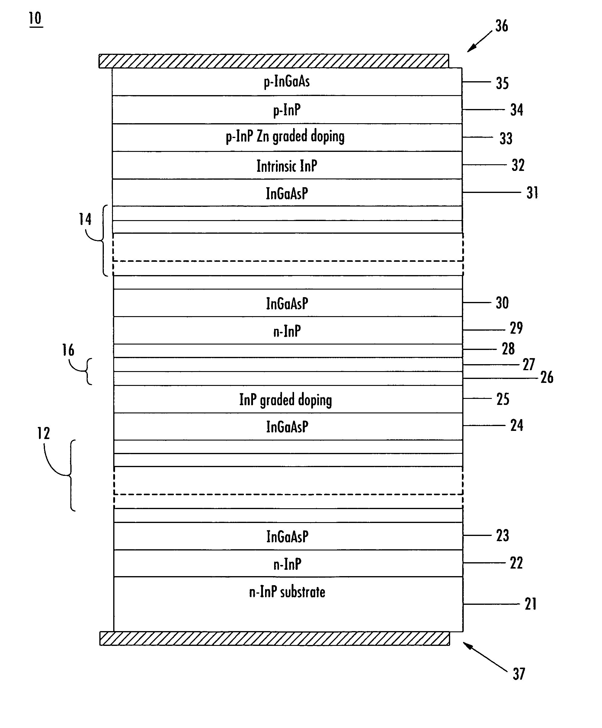
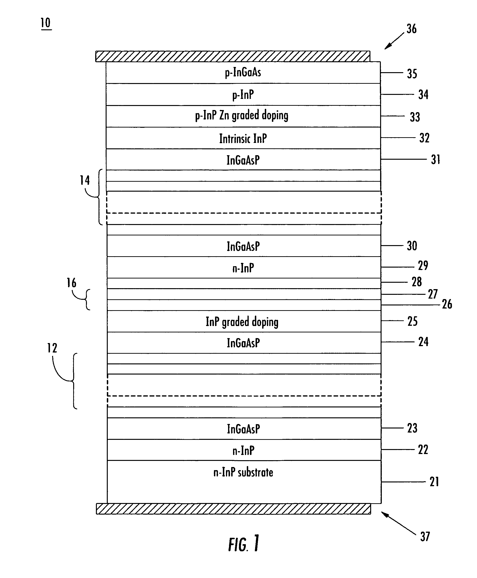
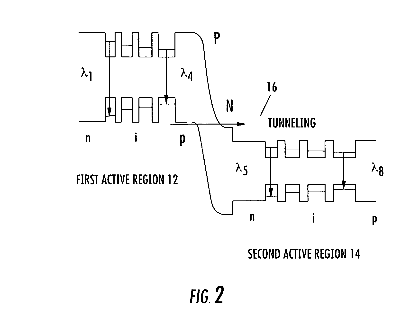
[0021]FIG. 1 is a schematic diagram of a multi-quantum well waveguide transverse structure 10 in accordance with the teachings of the present invention. Multi-quantum well waveguide transverse structure 10 comprises first active region 12 and second active region 14. Tunneling junction layer 16 is disposed between first active region 12 and second active region 14 making injection efficiency higher with transporting electrons through the whole quantum well regions. First active region 12 can comprise a plurality of quantum wells for providing a predetermined gain peak wavelength. For example, first active region 12 can comprise six quantum wells having a predetermined thickness for provi...


PUM


Abstract

A multi-quantum well optical waveguide structure comprises a plurality of active regions including quantum wells with different gain peak wavelengths to provide an ultra broadband optical gain spectrum. Two adjacent sets of active regions having a large band gap difference are connected by a tunneling injection layer to provide smooth electron transport. Single transverse-mode operation is obtained by narrowly tapering the width of the multi-quantum well optical waveguide from the center to the two ends. Higher-order modes are suppressed at the output of the tapered waveguide, even though the center waveguide portion supports higher-order modes. In this way, the multi- quantum well optical waveguide can be utilized for ultra broadband optical amplification using a single mode fiber.

Description

BACKGROUND OF THE INVENTION [0001] 1. Field of the Invention [0002] This invention relates to an optical waveguide to produce an ultra broadband optical gain which can be used for broadband optical amplifiers and ultra-broadly tunable lasers in optical wavelength division multiplexing (WDM) network systems. [0003] 2. Description of Related Art [0004] Semiconductor optical amplifiers and tunable lasers need broad band gain in order to fully utilize the advantage of optical WDM network systems. Quantum wells have been used in these devices to provide higher and broader optical gain. Multi-quantum (MQW) wells consisting of an identical composition and thickness can provide a typical gain spectrum of 60-70 . Conventional methods have been used to broaden the gain spectrum beyond this range, see S. Ikeda et al., “Semiconductor laser devices with a plurality of light emitting layers having different bands gaps and methods for driving the same” IEEE Photonics Technology Letters, Vol. 16, N...

Claims


Application Information

Patent Timeline
IPC IPC(8): H01S3/03
CPCB82Y20/00H01S5/026H01S5/1014H01S5/3095H01S2301/185H01S5/34373H01S5/4043H01S5/4087H01S2301/04H01S5/34306
Inventor CHOA, FOW-SENTANBUN-EK, TAWEE
Owner CHOA FOW SEN
Learn More