Method of fabricating nonvolatile semiconductor memory devices with uniform sidewall gate length

a semiconductor memory and sidewall gate technology, applied in semiconductor devices, instruments, electrical devices, etc., can solve the problems of scaling for the purpose of higher performance and integration approaching its limit, difficult to keep a capacitance coupling ratio, and complex structure, etc., to suppress the leakage of retained charge, good charge retention characteristic, and simple structur

Inactive Publication Date: 2006-10-19
RENESAS ELECTRONICS CORP
View PDF11 Cites 32 Cited by
  • Summary
  • Abstract
  • Description
  • Claims
  • Application Information

AI Technical Summary

Benefits of technology

[0007] The above-described floating gate method is widely used in a flash memory for storing a program for a mobile phone, a large-capacity flash memory for storing data, and others, and it is known to have good charge retention characteristic. However, along with the device scaling, it becomes difficult to keep a capacitance coupling ratio necessary for potential control of the floating gate, and the structure becomes complicated. Further, in order to suppress the leakage of retained charge, the thickness of a silicon oxide film surrounding the floating gate is required to be about 8 nm or more, and thus, the scaling for the purpose of higher performance and integration approaches its limit. Further, since a charge is stored in the conductive material of the floating gate, even if only one defect to be a leakage path exists in the silicon oxide film surrounding the floating gate, a charge retention time is extremely shortened.
[0008] In this point, since the MONOS keeps a charge in discrete trap in an insulating material, all the retained charges are not lost even if there are some leakage paths, and it is resistant to oxide film defects. Consequently, along with the device scaling, the MONOS method is considered advantageous because the thin oxide film even below 8 nm is applicable which is suitable for scaling, reliability prediction is facilitated since retention time is not extremely reduced due to the defect which occurs with low probability, and a memory cell structure is simple and is easily embedded with a logic circuit.
[0009] In the memory cell which adopts this MONOS method, as a split gate structure particularly suitable for scaling, there is the structure in which the memory MOS transistor (hereinafter referred to as “memory transistor”) is formed as a sidewall on the sidewall of the select MOS transistor (hereinafter referred to as “select transistor”) by utilizing a self align structure (Patent Document 1 and Non-Patent Document 2). In the case of this sidewall structure, since alignment margin for photolithography is not required and the gate length of the transistor formed by self align method can be reduced below the minimum resolution size of the photolithography, a smaller memory cell can be realized in comparison with the conventional structure which forms the adjacent two types of transistors by photomasks.

Problems solved by technology

However, along with the device scaling, it becomes difficult to keep a capacitance coupling ratio necessary for potential control of the floating gate, and the structure becomes complicated.
Further, in order to suppress the leakage of retained charge, the thickness of a silicon oxide film surrounding the floating gate is required to be about 8 nm or more, and thus, the scaling for the purpose of higher performance and integration approaches its limit.
Further, since a charge is stored in the conductive material of the floating gate, even if only one defect to be a leakage path exists in the silicon oxide film surrounding the floating gate, a charge retention time is extremely shortened.

Method used


Image

  • Method of fabricating nonvolatile semiconductor memory devices with uniform sidewall gate length
  • Method of fabricating nonvolatile semiconductor memory devices with uniform sidewall gate length
  • Method of fabricating nonvolatile semiconductor memory devices with uniform sidewall gate length

Examples


first embodiment

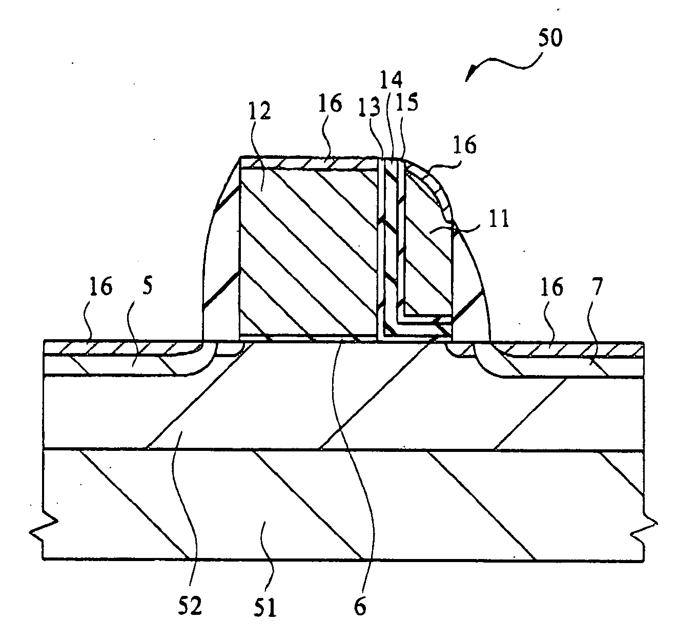
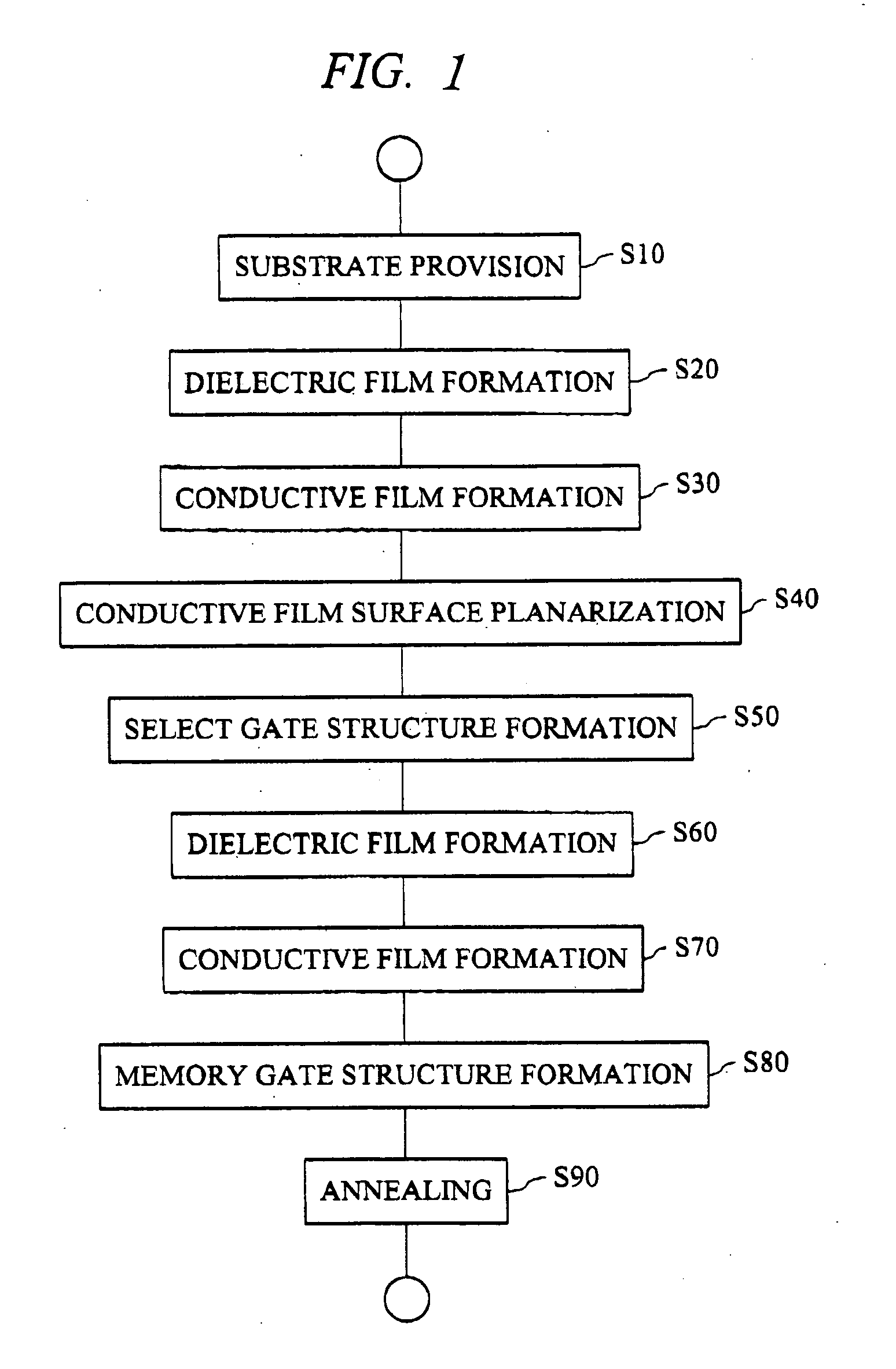
[0084] A fabricating method of a memory cell shown in a first embodiment of the present invention will be described with reference to FIG. 1 to FIG. 6. FIG. 1 is a fabrication flowchart of the memory cell shown in the first embodiment of the present invention, and FIG. 2 to FIG. 6 are explanatory drawings schematically showing the memory cell in the fabricating process. Note that the memory cell is a split gate MONOS memory cell shown in FIG. 17, an array structure is as shown in FIG. 18, and a cell layout is as shown in FIG. 19. A portion surrounded by dotted line 31 in FIG. 19 corresponds to unit memory cell. In adjacent cells, arrangement of a select gate and a memory gate is always symmetrical. Also, the voltage conditions of FIG. 20 are applied to the reading, programming, and erasing operations. Furthermore, a basic fabrication flow confirms to the method described in the “summary of the invention”. A process rule of 150 nm node is used for fabrication.

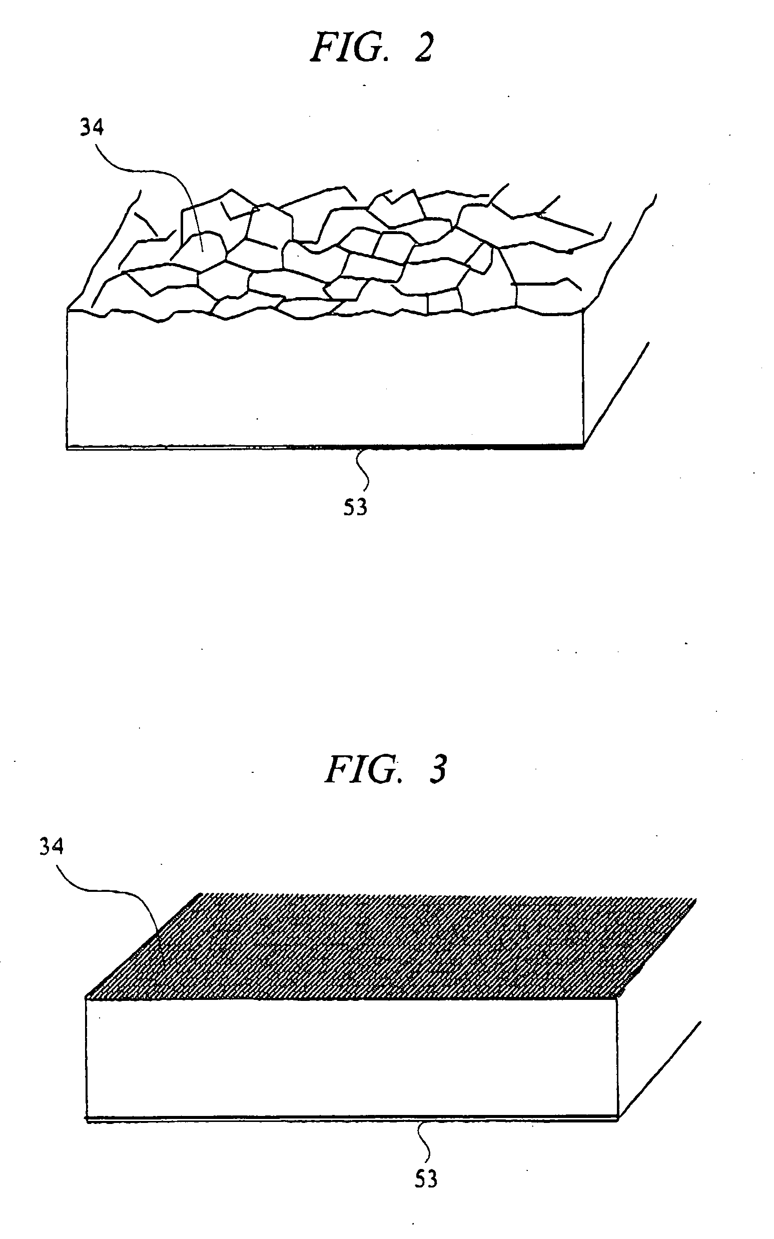
[0085] First, for examp...

second embodiment

[0096] In a second embodiment, the case where, after the conductive film of the gate electrode material made of polysilicon is formed in the fabricating process of the memory cell shown in the first embodiment, a cap layer made of SiO2 is formed thereon, and the cap layer made of SiO2 is planarized by CMP method will be described.

[0097] The fabricating method of a memory cell shown in the second embodiment of the present invention will be described with reference to FIG. 7 to FIG. 13. FIG. 7 is a fabrication flowchart of the memory cell shown in the second embodiment of the present invention, and FIG. 8 to FIG. 13 are explanatory drawings schematically showing the memory cell in the fabricating process. Note that the basic structure, layout, process rule and the like of the memory cell are the same as those of the first embodiment.

[0098] First, after a semiconductor substrate is prepared, a dielectric film and a conductive film are formed on the semiconductor substrate (not shown)...

third embodiment

[0108] In a third embodiment, the case where the gate length of the select transistor is set to 120 nm or more in the fabricating process of the memory cell shown in the first embodiment will be described.

[0109] The fabricating method of the memory cell shown in the third embodiment will be described with reference to FIG. 14 to FIG. 16. FIG. 14 is a fabrication flowchart of the memory cell shown in the third embodiment of the present invention, and FIG. 15 and FIG. 16 are explanatory drawings schematically showing the memory cell in the fabricating process. Note that the basic structure, layout, process rule and the like of the memory cell are the same as those of the first embodiment.

[0110] First, after a semiconductor substrate is prepared, a dielectric film and a conductive film are formed on the semiconductor substrate (steps S210 to S230). More specifically, a thermal oxide film with a thickness of 3 nm is formed as a dielectric film to be the gate dielectric film of a selec...


PUM


Abstract

After forming a first dielectric film on the main surface of a semiconductor substrate, a first conductive film is formed on the first dielectric film, and then, the surface of the first conductive film is planarized by a CMP method. Subsequently, the first conductive film and the first dielectric film are etched, thereby forming a select gate having a first gate electrode and a first gate dielectric film. Subsequently, after forming a second dielectric film on the sidewall of the first gate electrode and the main surface, a second conductive film is formed on the second dielectric film, and the second conductive film is etched, thereby forming a memory gate having a second gate electrode and a second gate dielectric film.

Description

CROSS-REFERENCE TO RELATED APPLICATION [0001] The present application claims priority from Japanese Patent Application No. JP 2005-119282 filed on Apr. 18, 2005, the content of which is hereby incorporated by reference into this application. TECHNICAL FIELD OF THE INVENTION [0002] The present invention relates to a method of fabricating a nonvolatile semiconductor memory device. More particularly, it relates to a technology effectively applied to the fabrication of a semiconductor nonvolatile memory cell. BACKGROUND OF THE INVENTION [0003] A nonvolatile semiconductor memory device can be realized as a high-performance semiconductor device by embedding a semiconductor nonvolatile memory cell (hereinafter referred to as “memory cell”) on the same semiconductor substrate together with a logic device such as a MOS transistor and others. This nonvolatile semiconductor memory device is widely used as an embedded microcomputer in industrial machines, home appliances, on-vehicle equipment, ...

Claims


Application Information

Patent Timeline
Patent Type & Authority Applications(United States)
IPC IPC(8): H01L21/336
CPCG11C16/0425G11C16/0466H01L21/28282H01L29/792H01L27/11568H01L29/42344H01L29/66833H01L27/105H01L29/40117H10B43/30
Inventor YASUI, KANKIMURA, SHINICHIROHISAMOTO, DIGHISHIMARU, TETSUYA
Owner RENESAS ELECTRONICS CORP
Why Eureka
Try Eureka