Using metal/metal nitride bilayers as gate electrodes in self-aligned aggressively scaled CMOS devices

a technology of metal/metal nitride bilayers and gate electrodes, which is applied in the direction of semiconductors, electrical devices, transistors, etc., can solve the problems of reducing the strength of the electric field at the surface, affecting the performance of the transistor, and the performance of the polysilicon gate may suffer device performance degradation, etc., to achieve high workfunction

Active Publication Date: 2006-10-26
TAIWAN SEMICON MFG CO LTD
View PDF6 Cites 63 Cited by
  • Summary
  • Abstract
  • Description
  • Claims
  • Application Information

AI Technical Summary

Benefits of technology

[0011] at least one pMOS device located on another region of said semiconductor substrate, where said at least one nMOS device includes a gate stack comprising at least a low workfunction elemental metal having a workfunction of ...

Problems solved by technology

However, polysilicon gates may suffer device performance degradation due to a polysilicon depletion effect in which an electric field applied to a polysilicon gate removes carriers (holes in a p-type doped polysilicon, or electrons in an n-type doped polysilicon) so as to create a depletion of carriers in the area of the polysilicon gate near the underlying gate dielectric of the transistor.
This depletion effect results in a reduction in the strength of the electric field at the surface of the CMOS device when a voltage is applied to the polysilicon gate electrode, which can have an adverse affect on the transistor performance.
While replacing traditional polysilicon gates with metal or metal alloy gate electrodes eliminates the polysilicon depletion effect, there are still problems associated with the use of such metal gates.
One problem encountered is that the carriers from the metal...

Method used


Image

  • Using metal/metal nitride bilayers as gate electrodes in self-aligned aggressively scaled CMOS devices
  • Using metal/metal nitride bilayers as gate electrodes in self-aligned aggressively scaled CMOS devices
  • Using metal/metal nitride bilayers as gate electrodes in self-aligned aggressively scaled CMOS devices

Examples


example

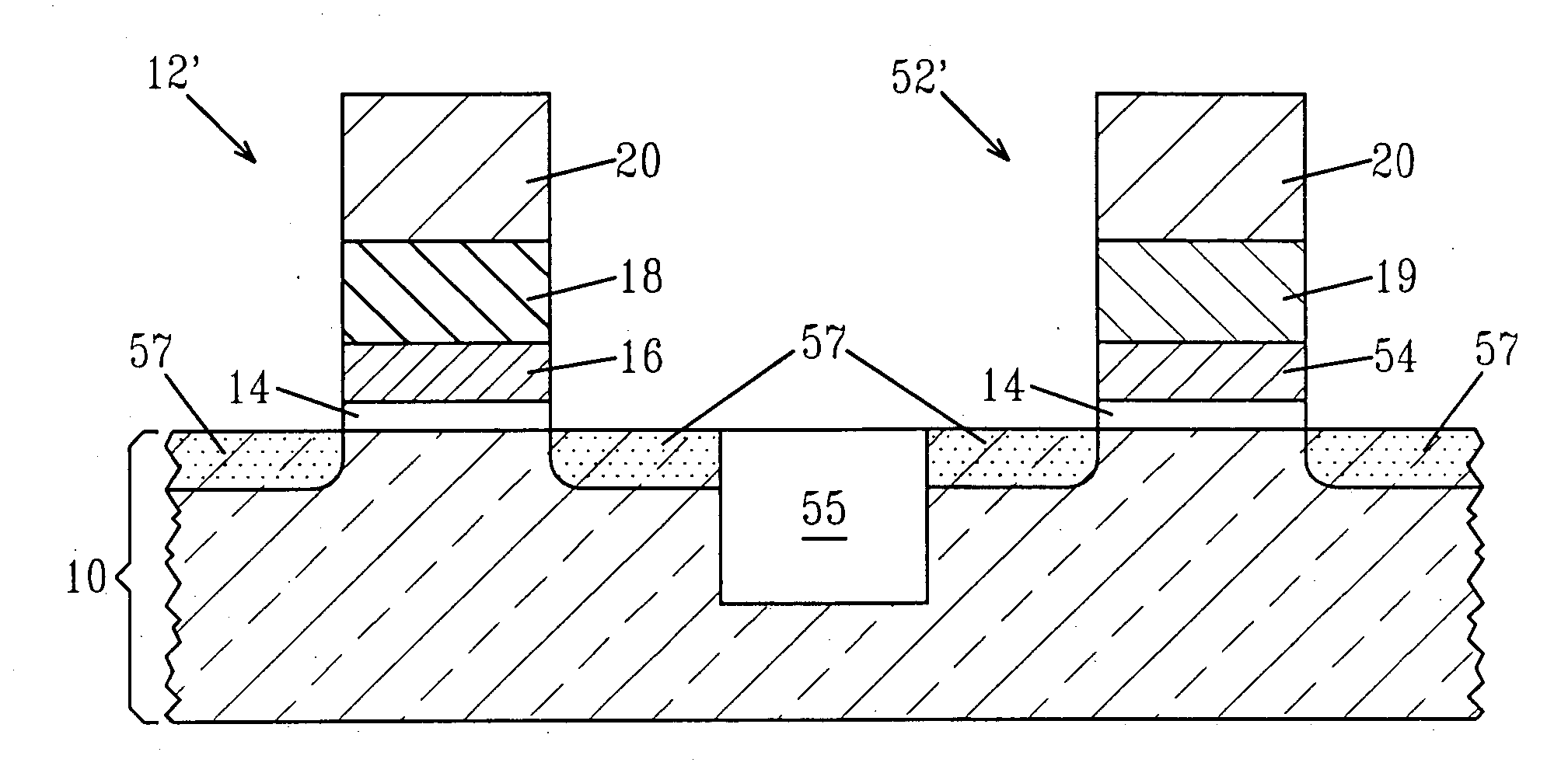
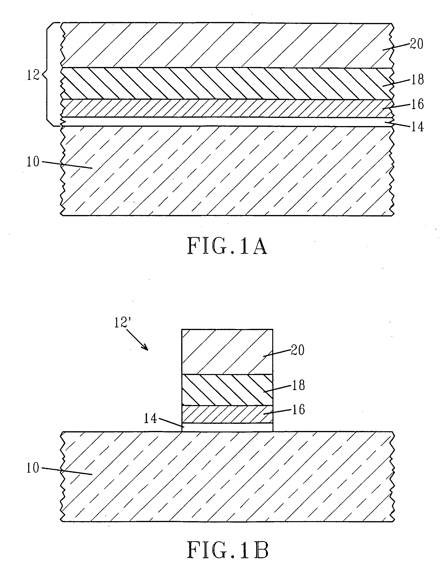
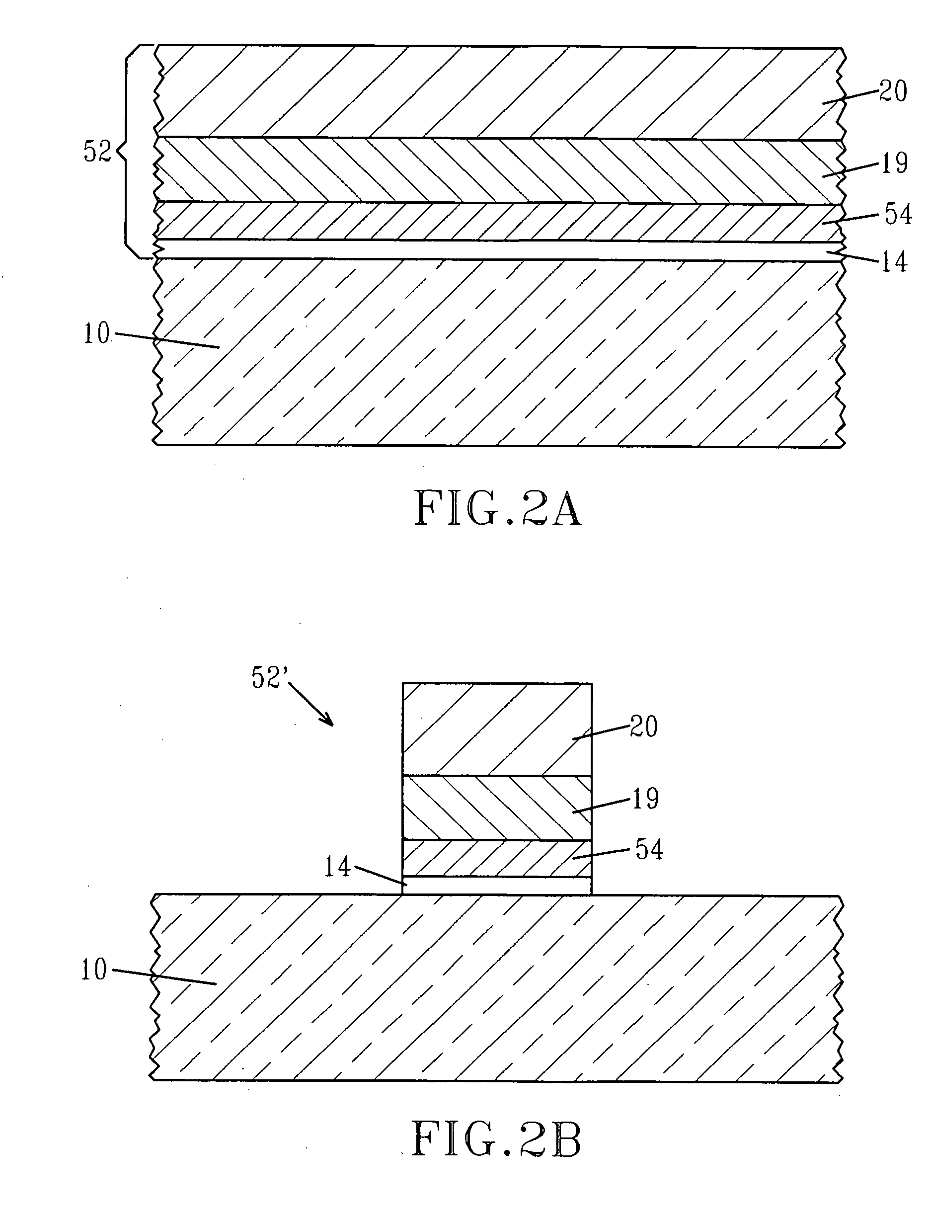
[0074] In the sole example of the present application, an nFET comprising Si / SiO2 / HfO2 / Ti / TiN / PolySi was prepared utilizing the basic processing steps described in the detailed description portion of the present invention. In this example, the deposition of the TiN capping layer was clustered to the deposition of the Ti (low workfunction elemental metal). Two gate stacks that were representative of the present invention were prepared; one including 10 Å Ti and 150 Å TiN, and the other including 20 Å Ti and 150 Å TiN. For comparison, an nMOS including TiN and an nMOS comprising polySi and SiON were also prepared.

[0075] Table 1 illustrates the effectiveness of the inventive nMOS structure after self-aligned MOSFET fabrication. The threshold voltage, Vt, the shift from mid-gap (towards nFET) and the inversion thickness, Tinv, are shown. The Vt and Tinv were measured using conventional techniques well known in the art. For example, the Vt was determined by calculating the current using...


PUM


Abstract

The present invention is directed to CMOS structures that include at least one nMOS device located on one region of a semiconductor substrate; and at least one pMOS device located on another region of the semiconductor substrate. In accordance with the present invention, the at least one nMOS device includes a gate stack comprising a gate dielectric, a low workfunction elemental metal having a worfunction of less than 4.2 eV, an in-situ metallic capping layer, and a polysilicon encapsulation layer and the at least one pMOS includes a gate stack comprising a gate dielectric, a high workfunction elemental metal having a workfunction of greater than 4.9 eV, a metallic capping layer, and a polysilicon encapsulation layer. The present invention also provides methods of fabricating such a CMOS structure.

Description

FIELD OF THE INVENTION [0001] The present invention relates to complementary metal oxide semiconductor (CMOS) structures and methods of forming the same. More particularly, the present invention provides a CMOS structure that includes an nMOS device that contains a low workfunction metal / metal nitride bilayer stack and a pMOS device that contains a high workfunction metal / metal nitride bilayer stack, wherein both nMOS and pMOS stacks remain stable during conventional high temperature self-aligned CMOS processing. BACKGROUND OF THE INVENTION [0002] As is known to those skilled in the semiconductor art, transistors are the main building blocks of integrated circuits (ICs). Modem ICs interconnect millions of densely configured transistors that perform a wide variety of functions. To achieve this densely packed configuration, the physical dimensions of the transistors are typically scaled down to the sub-micron regime. Generally, the transistors used in the sub-micron regime typically i...

Claims


Application Information

Patent Timeline
IPC IPC(8): H01L29/76
CPCH01L21/823842
Inventor CARTIER, EDUARD A.COPEL, MATTHEW W.DORIS, BRUCE B.JAMMY, RAJARAOKIM, YOUNG-HEELINDER, BARRY P.NARAYANAN, VIJAYPARUCHURI, VAMSI K.WONG, KEITH KWONG HON
Owner TAIWAN SEMICON MFG CO LTD
Why Eureka
Try Eureka