Junction barrier schottky with low forward drop and improved reverse block voltage

a technology of reverse block voltage and junction barrier, which is applied in the direction of basic electric elements, electrical apparatus, and semiconductor devices, can solve the problems of achieve the effect of improving performance and reducing the lateral dimension of the schottky devi

Inactive Publication Date: 2006-10-26
TAURUS MICROPOWER
View PDF4 Cites 46 Cited by
  • Summary
  • Abstract
  • Description
  • Claims
  • Application Information

AI Technical Summary

Benefits of technology

[0010] Specifically, it is an object of the present invention to provide a new device structure and manufacture method to provide new device structures and manufacture methods by implanting and then simultaneous diffusion of P and N ions into a drift N region supported on a N+ substrate. The forward barrier height is reduced while the reverse blocking voltage is increased. Furthermore, with a double diffusion process by either simultaneous or sequential diffusing the P-type and N-type ions reduces the effects of the lateral diffusion thus reduces the lateral dimension of the Schottky devices. More compact junction barrier devices are formed with improved performance are achieved by the disclosures made in this invention.

Problems solved by technology

Furthermore, with a double diffusion process by either simultaneous or sequential diffusing the P-type and N-type ions reduces the effects of the lateral diffusion thus reduces the lateral dimension of the Schottky devices.

Method used


Image

  • Junction barrier schottky with low forward drop and improved reverse block voltage
  • Junction barrier schottky with low forward drop and improved reverse block voltage
  • Junction barrier schottky with low forward drop and improved reverse block voltage

Examples


Embodiment Construction

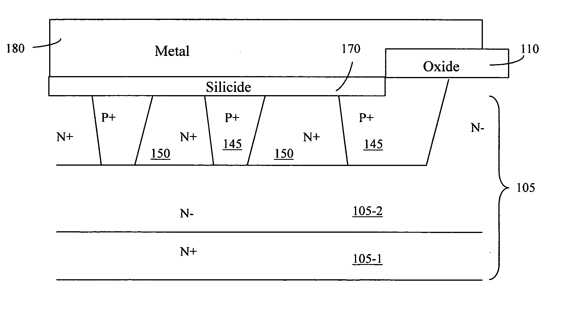
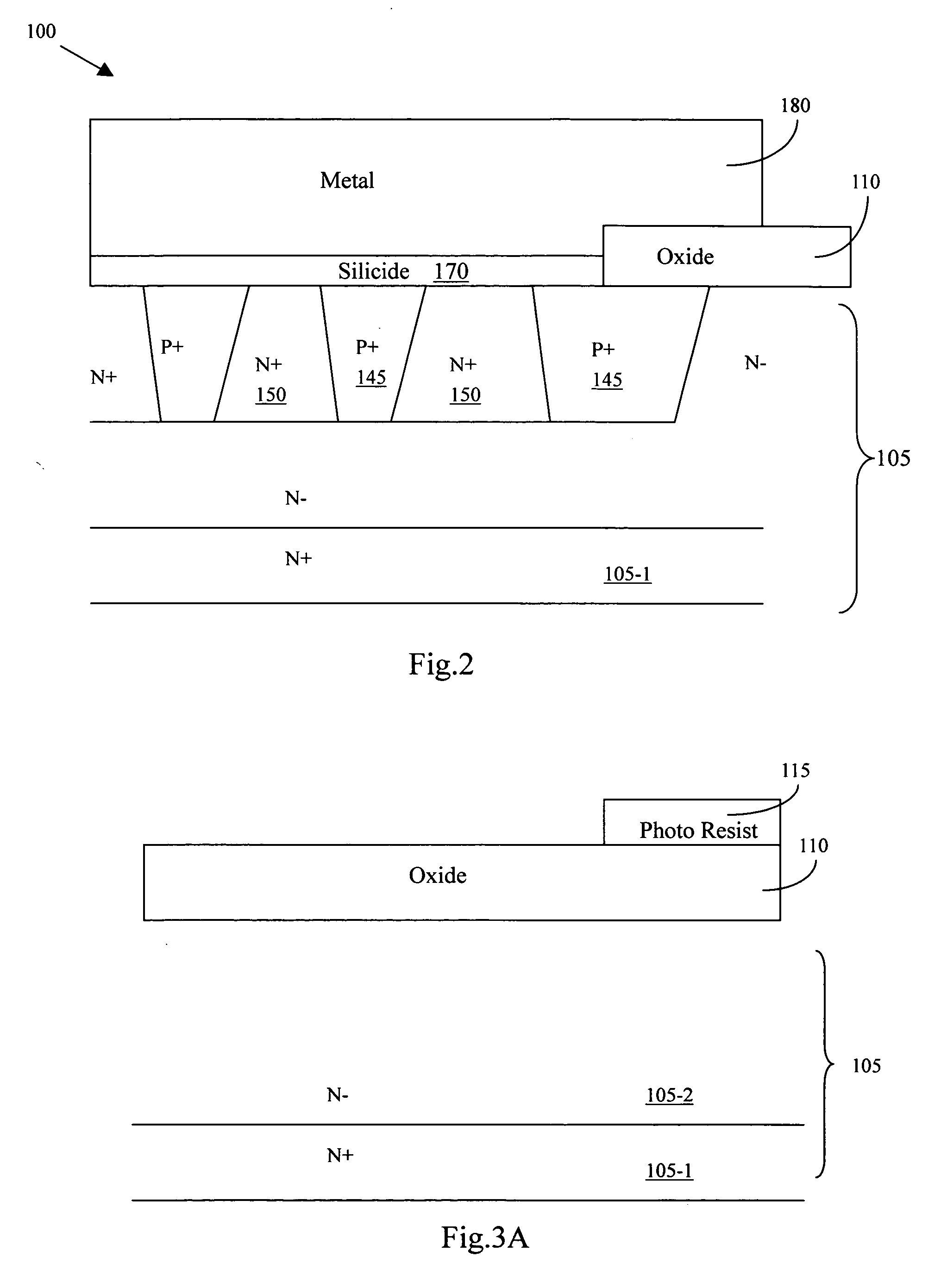
[0024] Referring now to FIG. 2 for a cross-sectional illustration of a first embodiment of a Schottky junction barrier device according to the present invention. The Schottky junction barrier device 100 is supported on a semiconductor substrate 105 of first conductivity type, typically N-type conductivity, having a first semiconductor layer 105-1 shown as N+ region and a second semiconductor layer 105-2 shown as N− region with impurity concentration lower than that of the first semiconductor layer 105-1. The Schottky junction barrier device further includes a metal layer 180 and a silicide layer 170 as Schottky contact to function as an anode of a diode. The junction barrier Schottky device further includes a plurality of P+ and N+ diffusion regions 145 and 150 respectively disposed adjacent to each other with prescribed width and intervals in an alternate sequence. The N+ diffusion regions 150 function as forward barrier reduction region while the P+ diffusion regions 145 function ...


PUM


Abstract

This invention discloses a junction barrier Schottky device supported on a substrate that has a first conductivity type. The Schottky device includes a first diffusion region of a fist conductivity type for functioning as a forward barrier height reduction region. The Schottky device further includes a second diffusion region of a second conductivity type disposed immediately adjacent to the first diffusion region for functioning as a backward blocking enhancement region to reduce the backward leakage current.

Description

BACKGROUND OF THE INVENTION [0001] 1. Field of the Invention [0002] This invention relates generally to the structure and fabrication process for manufacturing the junction barrier Schottky device. More particularly, this invention relates to a novel device structure and fabrication process for manufacturing junction barrier Schottky with low forward voltage drop and improved reverse block voltage. [0003] 2. Description of the Prior Art [0004] Even with excellent performance characteristics of a low forward voltage drop and fast reverse recovery period, the usefulness of a junction barrier Schottky device is still limited by several technical difficulties. A first technical limitation is the increase amount of reverse leakage current with the reduce junction barrier height. While a reduce junction barrier height provides an advantage of low forward conduction loss, it produces an associated side effect of increased reverse leakage current. Compared to common p-n junction diode, the ...

Claims


Application Information

Patent Timeline
Patent Type & Authority Applications(United States)
IPC IPC(8): H01L29/47
CPCH01L29/402H01L29/417H01L29/872H01L29/8611H01L29/66143
Inventor HSHIEH, FUW-IUANPRATT, BRIAN
Owner TAURUS MICROPOWER
Why Eureka
Try Eureka