

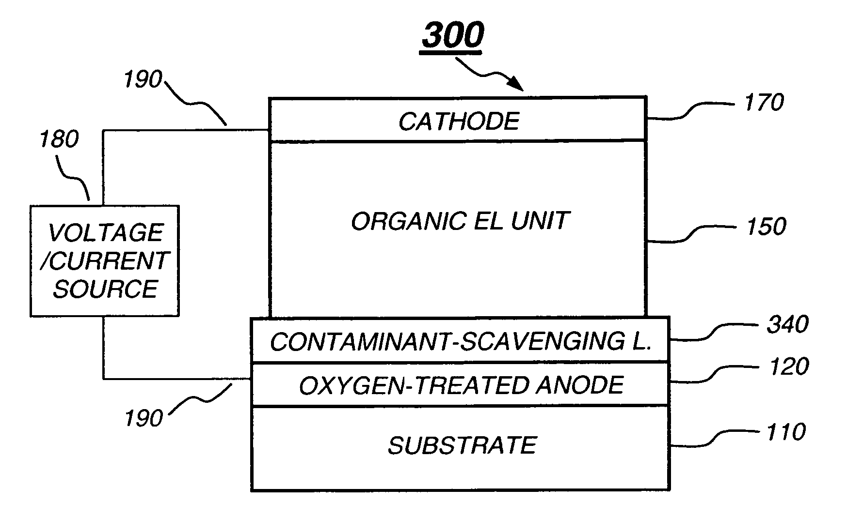
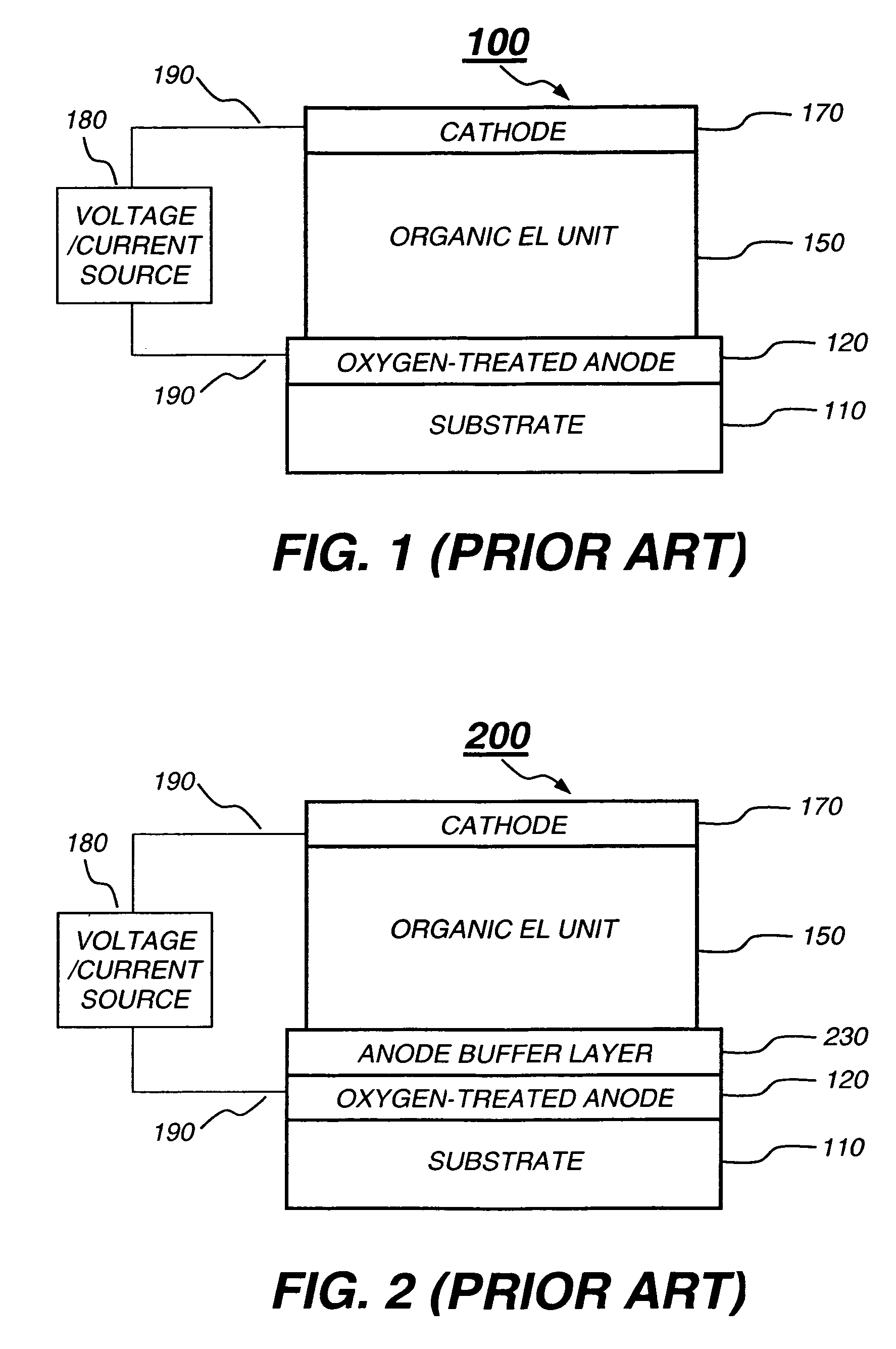
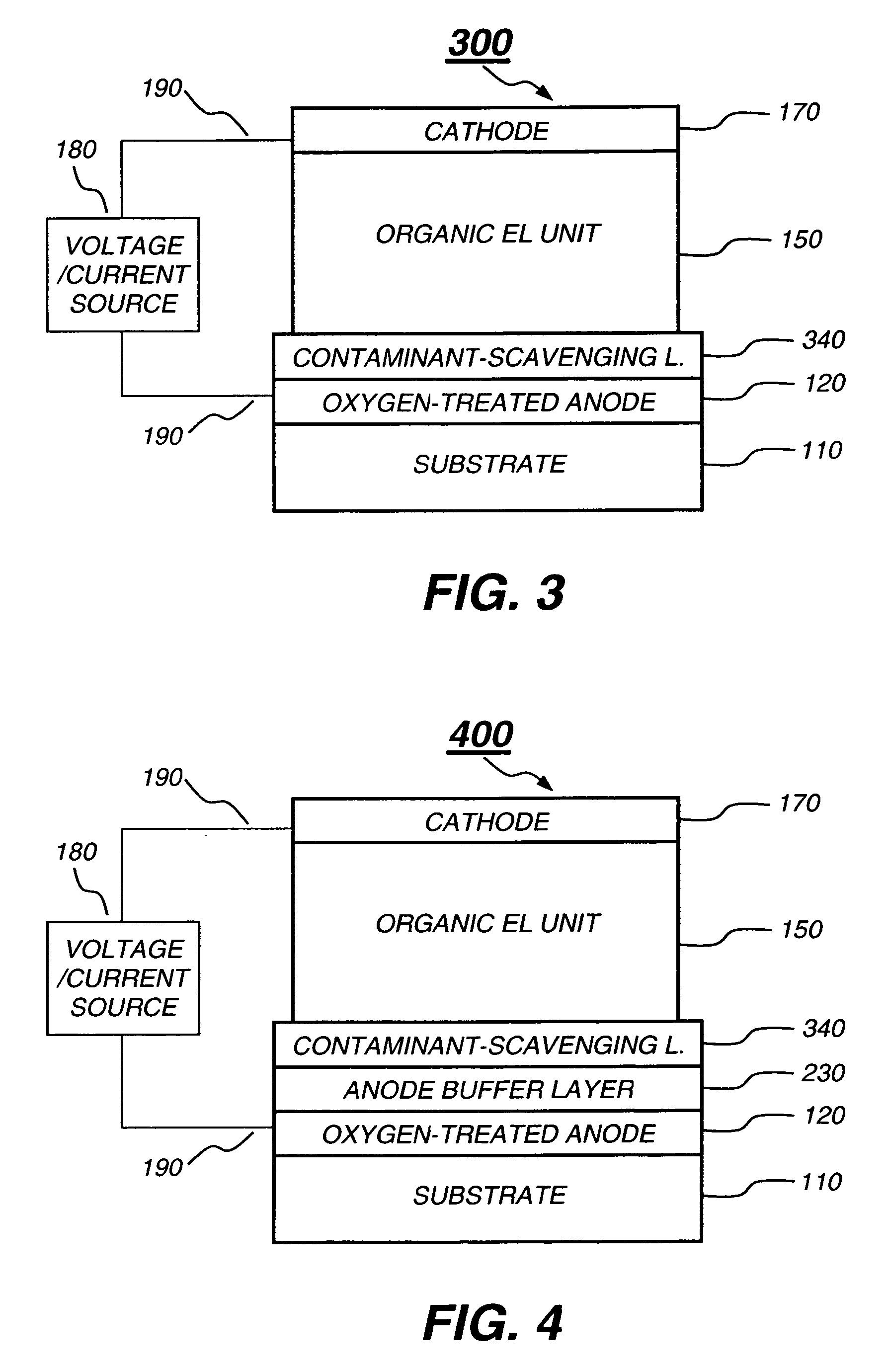
Contaminant-scavenging layer on OLED anodes
a technology of oled anodes and contaminant-scavenging layers, which is applied in the field of reducing, can solve the problems of contaminant contamination on the surface of clean anodes, surface contamination cannot be readily avoided even in vacuum chambers, and anodes that aren't contaminated before being transferred into vacuum chambers will become contaminated
- Summary
- Abstract
- Description
- Claims
- Application Information
AI Technical Summary
Benefits of technology
Problems solved by technology
Method used
Image

Examples
example 5
[0128] An OLED was constructed as the same as that in Example 4 with the same substrate waiting time (60 hours) and under the same environmental conditions, except that a 0.2 nm-thick contaminant-scavenging layer, F4-TCNQ layer, was deposited on top of the anode after the substrate waiting time and immediately before the formation of the organic EL unit. The reduction potential of F4-TCNQ was measured as about 0.64 V vs. SCE in the 1:1 MeCN / MePh organic solvent system.
[0129] This OLED requires a drive voltage of about 7.4 V to pass 20 mA / cm2. Under this test condition, the device has a luminance of 542 cd / m2, and a luminous efficiency of about 2.7 cd / A. Its emission peak is at 524 nm. The operational stability was measured as T80(70° C.@20 mA / cm2) which is longer than 200 hours. The EL performance data are summarized in Table 2.
TABLE 2Example(Type)WaitingWithLuminousEmissionT80(70° C. @(EL measured @TimeCSL*VoltageLuminanceEfficiencyPeak20 mA / cm2)20 mA / cm2)(Hrs)(nm)(V)(cd / m2)(cd / ...
example 7
[0134] An OLED was constructed as the same as that in Example 6 with the same substrate waiting time and under the same environmental conditions, except that a 0.4 nm-thick contaminant-scavenging layer, F4-TCNQ layer, was deposited on top of the anode after the substrate was exposed to the outgassing and pre-evaporation vacuum conditions and immediately before the formation of the organic EL unit.
[0135] This OLED requires a drive voltage of about 6.2 V to pass 20 mA / cm2. Under this test condition, the device has a luminance of 513 cd / M2, and a luminous efficiency of about 2.6 cd / A. Its emission peak is at 524 nm. The operational stability was measured as T90(RT@20 mA / cm2) which is longer than 350 hours. The EL performance data are summarized in Table 3.
TABLE 3Exposed toExample(Type)OrganicWithLuminousEmissionT90(RT @(EL measuredOutgassingCSL*VoltageLum.EfficiencyPeak20 mA / cm2)@ 20 mA / cm2)Environment(nm)(V)(cd / m2)(cd / A)(nm)(Hrs)6(Comparative)Yes07.44812.45282507Yes0.46.25132.6524>...
example 9
[0140] An OLED was constructed as the same as that in Example 8 with the same substrate waiting time and under the same environmental conditions, except that 1) a 0.5 nm-thick contaminant-scavenging layer, including hexanitrile hexaazatriphenylene, was deposited on top of the anode after the substrate was exposed to the outgassing and pre-evaporation vacuum conditions and immediately before the formation of the organic EL unit; and 2) the thickness of the HTL (NPB layer) in the organic EL unit was changed from 75 nm to 74.5 nm. The reduction potential of hexanitrile hexaazatriphenylene was measured as −0.08 V vs. SCE in the 1:1 MeCN / MePh organic solvent system.
[0141] This OLED requires a drive voltage of about 9.8 V to pass 20 mA / cm2. Under this test condition, the device has a luminance of 692 cd / m2, and a luminous efficiency of about 3.5 cd / A. Its emission peak is at 526 nm. The operational lifetime T50(RT@80 mA / cm2) is longer than 250 hours. The EL performance data are summarize...
PUM
| Property | Measurement | Unit |
|---|---|---|
| reduction potential | aaaaa | aaaaa |
| reduction potential | aaaaa | aaaaa |
| thickness | aaaaa | aaaaa |
Abstract
Description
Claims
Application Information