

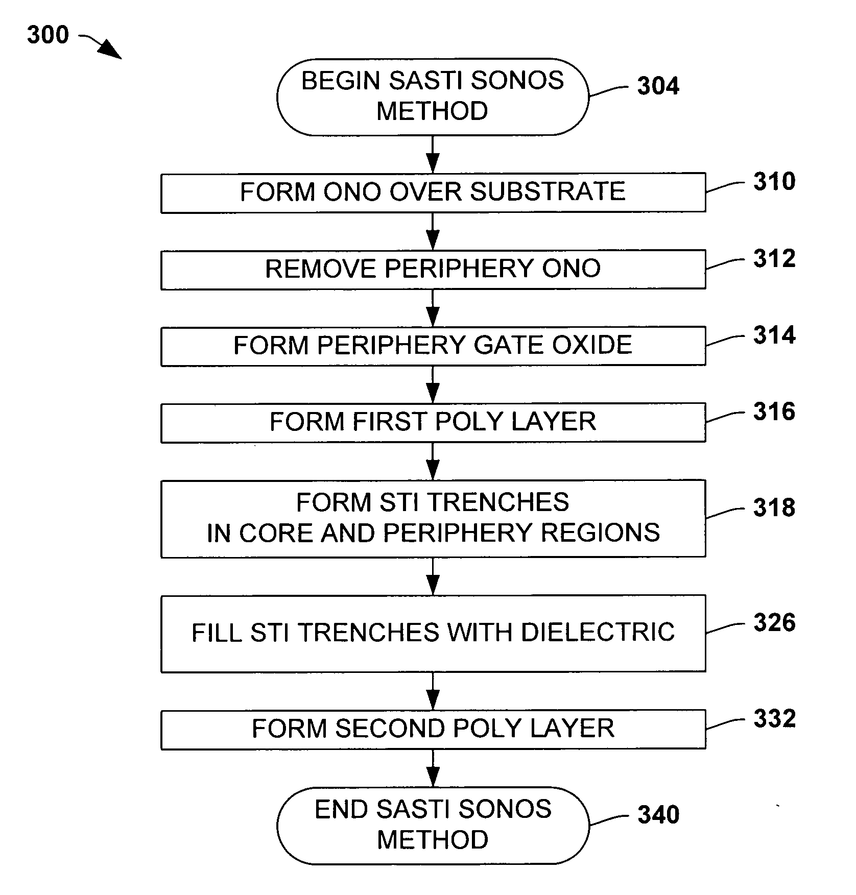
Self-aligned STI SONOS
a technology of sti sonos and self-aligning, which is applied in the field of self-aligning sti sonos, can solve the problems of limiting the designer's ability to reduce the dimensions of the cell, limiting the ability to scale the device within the desired performance specifications, and affecting the design's ability to reduce the cell's dimensions, etc., to achieve the effect of avoiding oxide thinning, facilitating the manufacture of scaled memory devices, and being difficult to remove conventional
- Summary
- Abstract
- Description
- Claims
- Application Information
AI Technical Summary
Benefits of technology
Problems solved by technology
Method used
Image

Examples
Embodiment Construction
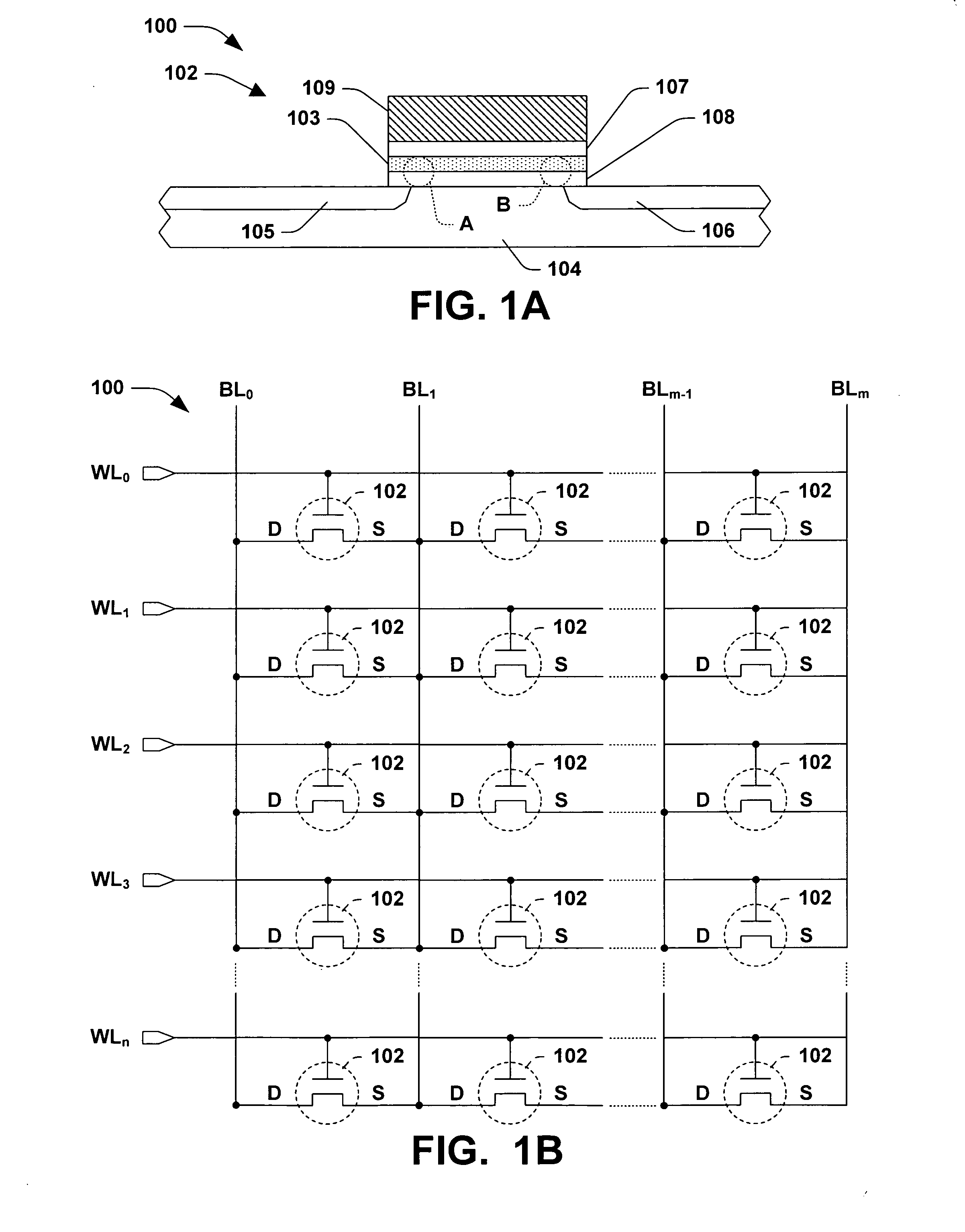
[0044] One or more implementations of the present invention will now be described with reference to the drawings, wherein like reference numerals are used to refer to like elements throughout, and wherein the various structures are not necessarily drawn to scale. The present invention relates to a system and method for fabricating flash memory structures and devices associated with dual-bit or other multi-bit SONOS type flash memory cells illustrated and described below. However, it will be appreciated that the invention may be employed in fabricating other types of flash memory devices, such as single and multi-bit cells, or others, and that the invention is not limited to the implementations specifically illustrated and described herein.
[0045] Referring initially to FIGS. 1A and 1B, such figures illustrate an exemplary dual bit memory cell 102 and a portion of a virtual ground memory array 100, respectively, including one or more interconnected cells 102 in one exemplary simplifi...
PUM
 Abstract
Description
Claims
Application Information