Design structure for coupling noise prevention

a design structure and noise prevention technology, applied in the field of integrated circuits, can solve problems such as noise generation in signal lines, affecting circuit functioning, and problems that will become worse in future generations, and achieve the effect of preventing coupling nois

Active Publication Date: 2006-11-02
TAIWAN SEMICON MFG CO LTD
View PDF13 Cites 16 Cited by
  • Summary
  • Abstract
  • Description
  • Claims
  • Application Information

AI Technical Summary

Benefits of technology

[0008] The preferred embodiments of the present invention provide a semiconductor structure for preventing coupling noise between chips, between integrated circuits in a chip and a method of forming the same.

Problems solved by technology

Due to cross talk, noise is generated in the signal lines and affects the functioning of the circuit.
The problem will become worse in future generations.
If not compensated for, coupling noise may cause signal delays, logic errors, and even circuit malfunctions.
Although the structure shown in FIG. 1 is simple from a design and manufacturability perspective, the cross talk isolation effect is not satisfactory.
In integrated circuits, space consumption is one of the major concerns.
The conventional solutions have significant space consumption; therefore, their usages are limited.
Adding grounded structures thus increases the complexity of the circuit design (e.g., may require additional metal layers).

Method used


Image

  • Design structure for coupling noise prevention
  • Design structure for coupling noise prevention
  • Design structure for coupling noise prevention

Examples


Embodiment Construction

[0025] The making and using of the presently preferred embodiments are discussed in detail below. It should be appreciated, however, that the present invention provides many applicable inventive concepts that can be embodied in a wide variety of specific contexts. The specific embodiments discussed are merely illustrative of specific ways to make and use the invention, and do not limit the scope of the invention.

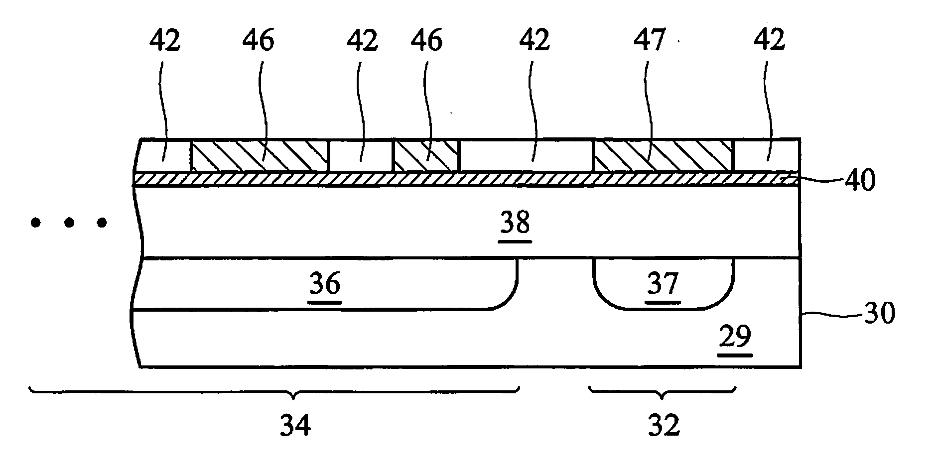
[0026] In an integrated circuit, metal lines may carry DC or AC current. Throughout the specification, metal lines carrying AC current are referred to as signal lines. Metal lines carrying signals with high current and high frequency have stronger cross talk with other lines. Cross talk is much more severe when the signal frequency is higher than about 1 GHz, and especially higher than about 3 GHz. The preferred embodiments of the present invention are preferably used for such high signal frequencies. The intermediate stages of manufacturing a preferred embodiment of the pr...


PUM


Abstract

A semiconductor structure for preventing coupling noise in integrated circuits and a method of forming the same are provided. The semiconductor structure includes a signal-grounded seal ring. The seal ring includes a plurality of metal lines, each in a respective metal layer and surrounding a circuit region of the semiconductor chip, a plurality of vias connecting respective metal lines, and a plurality of dielectric layers isolating each metal layer from any other metal layers. The seal ring may further include additional seal rings formed inside or outside the seal ring. The semiconductor structure may include laser fuses and protective rings. The protective rings are preferably signal grounded. Cross talk between sub circuits in a chip can be reduced by forming a seal ring extension between the sub circuits.

Description

TECHNICAL FIELD [0001] This invention relates generally to the formation of integrated circuits, and more specifically to the prevention of cross talk between signal lines. BACKGROUND [0002] Interference, or cross talk, occurs between two closely spaced signal lines. The cross talk is caused by electromagnetic fields generated by the signal lines. Due to cross talk, noise is generated in the signal lines and affects the functioning of the circuit. [0003] The problem will become worse in future generations. Due to the scaling down of device geometries in deep-sub-micron technologies, interconnect wires are placed in increasingly closer proximity and higher density. With increased use of stacked dies and system in package (SIP) technologies, cross talk between chips increases significantly due to the small distance between chips. As a result of the increasing circuit density, coupling noise has increased significantly, and has become an important concern in high performance circuit de...

Claims


Application Information

Patent Timeline
Patent Type & Authority Applications(United States)
IPC IPC(8): H01L23/34
CPCH01L23/5225H01L23/5258H01L2924/0002H01L2924/00
Inventor CHEN, HSIEN-WEICHEN, HSUEH-CHUNG
Owner TAIWAN SEMICON MFG CO LTD
Why Eureka
Try Eureka