
Light-emitting layer spacing in tandem OLED devices

a technology of tandem oled and light-emitting layer, which is applied in the direction of discharge tube luminescnet screen, discharge tube/lamp details, electric discharge lamps, etc. it can solve the problems of high operating voltage, high angle dependence of devices, and difficulty in including white light-emitting units in tandem oled structures, etc., to reduce the thickness of the layer, improve light output, and operate at a lower voltage

Inactive Publication Date: 2006-11-02
EASTMAN KODAK CO
View PDF21 Cites 55 Cited by
  • Summary
  • Abstract
  • Description
  • Claims
  • Application Information

AI Technical Summary

Benefits of technology

[0012] An advantage of the present invention is that it enables a reduction of the layer thickness used in constructing a tandem OLED device resulting in a lower operating voltage.

Problems solved by technology

However, each OLED unit in their devices needs a separate power source.
These tandem OLED devices, however, have a problem of high operating voltage, not only because the voltage of all the individual EL units adds up, but because of the large thickness of all the layers used.
These devices also suffer high angle dependence in their output.
It also has been difficult to include white light-emitting units in a tandem OLED structure.

Method used


Image

  • Light-emitting layer spacing in tandem OLED devices
  • Light-emitting layer spacing in tandem OLED devices
  • Light-emitting layer spacing in tandem OLED devices

Examples


Embodiment Construction

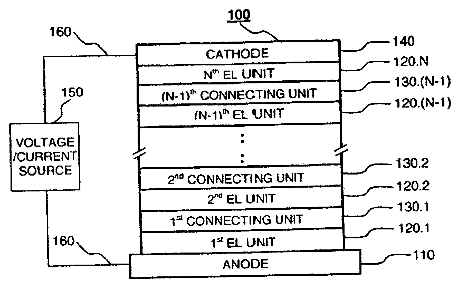
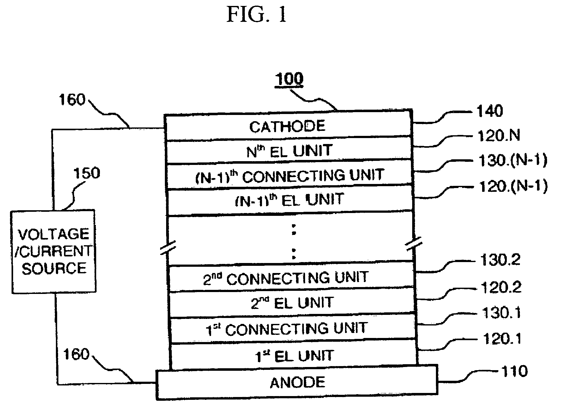
[0025]FIG. 1 shows a tandem OLED 100 in accordance with the present invention. This tandem OLED has an anode 110 and a cathode 140, at least one of which is transparent. Disposed between the anode and the cathode are N organic EL units 120, where N is an integer greater than 1. These organic EL units, connected serially to each other and to the anode and the cathode, are designated 120.1 to 120.N where 120.1 is the first EL unit (adjacent to the anode) and120.N is the Nth unit (adjacent to the cathode). The term EL unit 120 represents any of the EL units named from 120.1 to 120.N in the present invention. When N is greater than 2, there are organic EL units not adjacent to the anode or cathode, and these can be referred to as intermediate organic EL units. Disposed between any two adjacent organic EL units is a connecting unit 130. There are a total of N−1 connecting units associated with N organic EL units and they are designated 130.1 to 130.(N-1). Connecting unit 130.1 is dispose...


PUM


Abstract

A tandem organic electroluminescent device includes an anode and a cathode. The device also includes a plurality of organic electroluminescent units disposed between the anode and the cathode, wherein each of the organic electroluminescent units includes one or more organic layers including at least a light-emitting layer and an associated light-emitting junction, connecting unit disposed between adjacent organic electroluminescent units, and wherein at least two of the neighboring light-emitting junctions are separated by a distance of less than 90 nanometers.

Description

CROSS-REFERENCE TO RELATED APPLICATION [0001] Reference is made to commonly assigned U.S. patent application Ser. No. 10 / 437,195 filed May 13, 2003 by Liang-Sheng L. Liao et al., entitled “Cascaded Organic Electroluminescent Device Having Connecting Units With n-Type and p-Type Organic Layers” (U.S. Patent Application Publication 2004 / 0227460 A1), the disclosure of which is herein incorporated by reference. FIELD OF INVENTION [0002] The present invention relates to providing a plurality of organic electroluminescent (EL) units to form a tandem organic electroluminescent device. BACKGROUND OF THE INVENTION [0003] Organic electroluminescent (EL) devices or organic light-emitting devices (OLEDs) are electronic devices that emit light in response to an applied potential. The structure of an OLED includes, in sequence, an anode, an organic EL medium, and a cathode. The organic EL medium disposed between the anode and the cathode commonly includes an organic hole-transporting layer (HTL) ...

Claims


Application Information

Patent Timeline
IPC IPC(8): H01L51/00
CPCH01L51/5278H01L51/5265H10K50/19H10K59/876H10K50/852
Inventor TYAN, YUAN-SHENGFARRUGGIA, GIUSEPPE
Owner EASTMAN KODAK CO
Learn More