INTERCONNECT STRUCTURE ENCASED WITH HIGH AND LOW k INTERLEVEL DIELECTRICS

a technology of interconnections and dielectrics, applied in the direction of semiconductor devices, electrical apparatus, semiconductor/solid-state device details, etc., can solve the problems of significant esd failure mechanism of aluminum interconnects, inconvenient application of interconnects surrounded by low-k materials, etc., to improve the critical current density-to-failure robustness, improve the esd robustness of semiconductor chips, and increase the esd robustness of interconnects

Active Publication Date: 2006-11-09
TAIWAN SEMICON MFG CO LTD
View PDF4 Cites 3 Cited by
  • Summary
  • Abstract
  • Description
  • Claims
  • Application Information

AI Technical Summary

Benefits of technology

[0010] It is an advantage of the present invention to provide an interconnect structure that improves the ESD robustness of semiconductor chips.
[0011] It is a further advantage of the present invention to provide an interconnect structure that allows thermal heat to penetrate a short distance into the surrounding insulators of the interconnect between an ESD device and a pad to increase the ESD robustness of the interconnect.
[0012] It is a further advantage of the present invention to provide an interconnect structure that has an improved critical current density-to-failure robustness without increasing the capacitance of the interconnect.
[0013] The present invention is directed to a semiconductor structure having an ESD device and a receiver network connected to a pad by interconnects. The interconnect between the pad and the ESD device has a high-k material placed on at least one edge or surface of the interconnect within the thermal diffusion distance of the interconnect on an ESD pulse time scale. The high-k material improves the critical current density of the interconnect by increasing the heat capacity and thermal conductivity of the interconnect. The high-k material can be placed on the sides, top and / or bottom of the interconnect extending between the pad and the ESD device to improve the ESD robustness. In multiple wire interconnects extending between the pad and the ESD device, the high-k material is placed between the wires of the interconnect.
[0014] A low-k material is placed beyond the high-k material (i.e., beyond the thermal diffusion distance of the interconnect) to reduce the capacitance of the interconnect. The combination of low-k and high-k materials provides an interconnect structure with improved ESD robustness and low capacitance that is well suited for connecting the pad to the ESD device. The interconnect to the receiver, which is a functional circuit that does not carry a high current, is surrounded by a low-k material for reduced capacitance and performance advantages. Since this interconnect does not carry a high current, ESD robustness is much less of a concern than capacitance and performance.
[0015] According to a broad aspect of the present invention, an integrated circuit apparatus is provided, comprising: an electrostatic (ESD) device; a pad; an interconnect electrically connecting the pad and the ESD device; a high-k material placed adjacent to at least one surface of the interconnect for increasing an electrostatic discharge robustness of the interconnect; and a low-k material placed adjacent to the high-k material for reducing a capacitance of the interconnect.

Problems solved by technology

Aluminum interconnects are a significant ESD failure mechanism in high-pin-count microprocessor chips.
However, the interconnects surrounded by low-k materials are not well suited for applications where ESD robustness is more important than performance, such as interconnects between pads and ESD devices or other devices for discharging or sinking a current.

Method used


Image

  • INTERCONNECT STRUCTURE ENCASED WITH HIGH AND LOW k INTERLEVEL DIELECTRICS
  • INTERCONNECT STRUCTURE ENCASED WITH HIGH AND LOW k INTERLEVEL DIELECTRICS
  • INTERCONNECT STRUCTURE ENCASED WITH HIGH AND LOW k INTERLEVEL DIELECTRICS

Examples


Embodiment Construction

[0043] A preferred embodiment of the present invention will now be described with reference to the accompanying drawings.

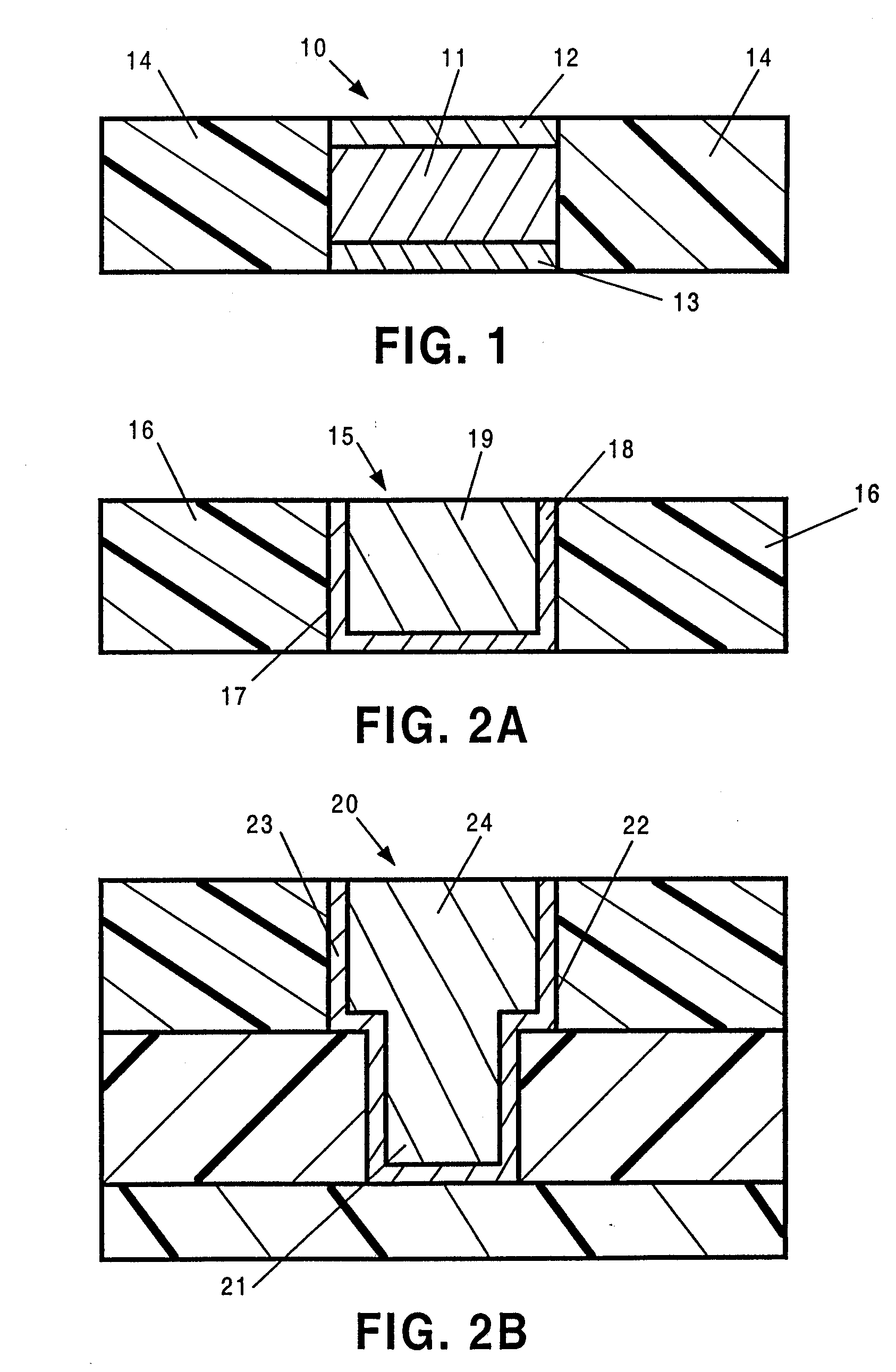
[0044] The present invention is directed to improvements in interconnect structures used in semiconductor devices. Such interconnect structures typically have one or more conductor wires, such as aluminum (Al) or copper (Cu) wires, surrounded by insulator materials. FIG. 1 shows a cross section of an Al-based interconnect 10 having a layer 11 of Al sandwiched between upper and lower layers 12, 13 of a refractory metal, such as titanium (Ti) or titanium nitride (TiN). An insulator material 14 is disposed on the sides of the interconnect 10.

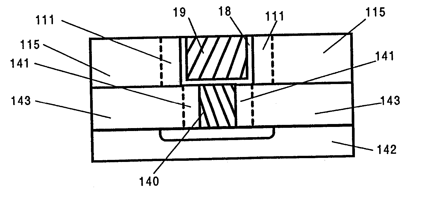
[0045]FIG. 2A shows a cross section of a Cu-based interconnect 15 having a damascene structure. The interconnect 15 has an insulator 16 in which a trough 17 is formed by a reactive ion etching process or the like. A liner 18 is deposited on the surface of the trough 17. A copper material 19 is then deposited on top of the liner...


PUM


Abstract

A structure for improving the electrostatic discharge robustness of an integrated circuit having an electrostatic discharge (ESD) device and a receiver network connected to a pad by interconnects. The interconnect between the pad and the ESD device has a high-k material placed adjacent to at least one surface of the interconnect and extending over the thermal diffusion distance of the interconnect. The high-k material improves the critical current density of the interconnect by increasing the heat capacity and thermal conductivity of the interconnect. The high-k material can be placed on the sides, top and / or bottom of the interconnect. In multiple wire interconnects, the high-k material is placed between the wires of the interconnect. A low-k material is placed beyond the high-k material to reduce the capacitance of the interconnect. The combination of low-k and high-k materials provides an interconnect structure with improved ESD robustness and low capacitance that is well suited for an ESD device. The interconnect to the receiver, which does not carry a high current, is surrounded by a low-k material for reduced capacitance and performance advantages.

Description

FIELD OF THE INVENTION [0001] The present invention relates generally to interconnects for electrostatic discharge (ESD) networks and receiver networks. More particularly, the present invention relates to structures for improving the thermal conductivity and ESD robustness of such interconnects by encasing the interconnects in a combination of high-k and low-k interlevel dielectric (ILD) materials. BACKGROUND OF THE INVENTION [0002] Semiconductor devices are typically interconnected by patterned electrically conductive layers of high conductivity metal or metal alloy, commonly referred to as interconnects or interconnect wires. Complex circuits require very close spacing of interconnect wires and multiple levels of metalization to interconnect the semiconductor devices. Interconnects are made by depositing and patterning alternating layers of a conductive material and layers of an insulating dielectric material. In multilevel interconnects, small holes or contact vias are formed thr...

Claims


Application Information

Patent Timeline
Patent Type & Authority Applications(United States)
IPC IPC(8): H01L29/76H01L29/94H01L31/00
CPCH01L23/485H01L23/53295H01L2924/0002H01L2924/00
Inventor VOLDMAN, STEVEN H.
Owner TAIWAN SEMICON MFG CO LTD
Why Eureka
Try Eureka