Reflective-type mask blank for EUV lithography and method for producing the same

a technology of euv lithography and mask blank, which is applied in the direction of photomechanical treatment originals, instruments, nuclear engineering, etc., can solve the problems of loss of sharpness, adversely affecting profile accuracy and dimensional accuracy, and conventional exposure techniques using light exposure close to the limit, etc., to achieve excellent contrast ratio, excellent contrast ratio, and high precision

Inactive Publication Date: 2006-11-09
ASAHI GLASS CO LTD
View PDF3 Cites 104 Cited by
  • Summary
  • Abstract
  • Description
  • Claims
  • Application Information

AI Technical Summary

Benefits of technology

[0021] In the mask blank of the present invention, the absorbing layer is a Cr layer deposited by an ion beam sputtering method whereby the reflectance of EUV ray at the absorbing layer can be reduced. Preferably, the reflectance of EUV ray at the absorbing layer is 0.1% or less. By reducing the EUV ray reflectance at the absorbing layer, it is possible to provide an excellent contrast ratio of the EUV ray reflectance at the reflective layer to that at the absorbing layer, preferably, the contrast ratio of the EUV ray reflectance at the reflective layer to that at the absorbing layer is 600 / 1 or more. Thus, by conducing EUV lithography employing the reflective-type photomask having excellent contrast ratio, it is possible to form a pattern of high precision on a semiconductor substrate.
[0022] According to the method for producing a mask blank according to the present invention, the mask blank of the present invention wherein the EUV ray reflectance at the absorbing layer is 0.1% or less can be produced. Here, the EUV ray reflectance at the absorbing layer means the reflectance of the reflective layer to the ray having the center wavelength of EUV light in the reflectance profile of the reflective layer in a case that a ray in the wavelength region of the EUV light is incident into the surface of the absorbing layer at an incident angle in a range of 2 to 100.

Problems solved by technology

However, the conventional exposure techniques using light exposure have been close to the limit while semiconductor devices have had finer patterns at an accelerated pace.
However, a thick absorbing layer causes a problem when a pattern is printed on a semiconductor substrate by employing a reflective-type photomask.
Therefore, when the thickness of the mask pattern formed by dry-etching an absorbing layer is large, the shadow of the mask pattern is produced to thereby adversely affect the profile accuracy and the dimensional accuracy, and the pattern image reflected during the exposure of light loses its sharpness whereby the dimensional accuracy of the pattern is deteriorated.
Accordingly, there is further limitation on the thickness of the absorbing layer.

Method used


Image

  • Reflective-type mask blank for EUV lithography and method for producing the same
  • Reflective-type mask blank for EUV lithography and method for producing the same
  • Reflective-type mask blank for EUV lithography and method for producing the same

Examples


examples

[0078] In the following, the present invention will be described with Examples.

example

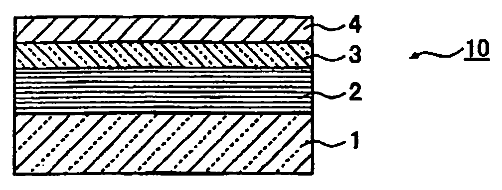
[0079] In this Example, the mask blank shown in FIG. 1 was prepared by the following process.

Formation of Reflective Layer

[0080] In this Example, a SiO2-TiO2 type glass substrate 1 (having outer dimensions of 6 inch (152.4 mm) square and a thickness of 6.3 mm) was used. This glass substrate 1 has a thermal expansion coefficient of 0.2×10⁻⁷ / ° C. and a Young's modulus of 67 GPa. The glass substrate 1 was polished so that the surface having a surface roughness Rms of 0.2 nm or less and a flatness of 100 nm or less was formed.

[0081] On the surface of the glass substrate 1, a Si film and a Mo film were deposited alternately in 40 cycles by an ion beam sputtering method, whereby a Mo / Si reflective film (reflective layer 2) having a total film thickness of 272 nm ((4.5±2.3)×40) was formed. Finally, a Si layer was deposited to have a film thickness of 11.0 nm as a capping layer.

[0082] Conditions of depositing the Si film and the Mo film were as follows.

Conditions of Depositing Si Fil...


PUM

PropertyMeasurementUnit
thicknessaaaaaaaaaa
thicknessaaaaaaaaaa
thicknessaaaaaaaaaa

Abstract

A reflective-type mask blank for EUV lithography for reducing the EUV ray reflectance at the absorbing layer and a method for producing the mask blank are presented. A reflective-type mask blank for EUV lithography comprising a substrate and a reflective layer for reflecting EUV light and an absorbing layer for absorbing EUV light, which are formed on the substrate in this order, the reflective-type mask blank for EUV lithography being characterized in that the absorbing layer is a Cr layer of low EUV ray reflectance deposited by an ion beam sputtering method.

Description

TECHNICAL FIELD [0001] The present invention relates to a reflective-type mask blank for EUV (extreme ultraviolet) lithography used for producing a semiconductor or the like and a method for producing the mask blank. BACKGROUND ART [0002] In the semiconductor industry, a photolithography method using visible light or ultraviolet light has been employed as a technique for writing, on a Si substrate or the like, a fine pattern, which is required for writing an integrated circuit comprising such a fine pattern. However, the conventional exposure techniques using light exposure have been close to the limit while semiconductor devices have had finer patterns at an accelerated pace. In the case of light exposure, it is said that the resolution limit of a pattern is about ½ of exposure wavelength, and even if an F2 laser (157 nm) is employed, it is estimated that the resolution limit is about 70 nm. From this point of view, EUV lithography which is an exposure technique using EUV light hav...

Claims


Application Information

Patent Timeline
Patent Type & Authority Applications(United States)
IPC IPC(8): G21K5/00B32B9/00B32B17/06G03F1/00G03F1/22G03F1/24G03F1/54
CPCC03C17/3649C03C17/3639C03C2217/734C03C2218/156C03C2218/33C23C14/46G03F1/22G03F1/24G03F1/54G21K1/062G21K2201/067B82Y10/00B82Y40/00C03C17/36C03C17/3615C03C17/3665
Inventor TAKAKI, SATORUHAYASHI, KAZUYUKI
Owner ASAHI GLASS CO LTD
Why Eureka
Try Eureka