Method for fabricating electrically connecting structure of circuit board

a technology of electrical connection and circuit board, which is applied in the direction of printed circuit manufacturing, printed circuit aspects, non-metallic protective coating applications, etc., can solve the problems of increasing stencil cost, material, limiting the passing of solder, etc., and achieves cost increase

Inactive Publication Date: 2006-11-09
PHOENIX PRECISION TECH CORP
View PDF0 Cites 28 Cited by
  • Summary
  • Abstract
  • Description
  • Claims
  • Application Information

AI Technical Summary

Benefits of technology

[0010] In views of the above-mentioned problems of the prior art, it is a primary objective of the present invention to provide a method for fabricating an electrically connecting structure of...

Problems solved by technology

However, too small the openings not only increase the cost of the stencil, but also restrict the passing of solder, material, forming a manufacturing bottleneck.
Moreover, that the solder materials are required to be formed in the openings so accurately not only ensures the correctness of size of the stencil, but also closely relates to a cleaning problem of the stencil printing technique.
Therefore, the stencil has to be cleaned completely every time the printing process is applied by the stencil printing technique on the stencil, this complicating a manufacturing process and reducing the reliability of the ...

Method used


Image

  • Method for fabricating electrically connecting structure of circuit board
  • Method for fabricating electrically connecting structure of circuit board
  • Method for fabricating electrically connecting structure of circuit board

Examples


Embodiment Construction

[0027] The following illustrative embodiments are provided to illustrate the disclosure of the present invention, these and other advantages and effects can be apparently understood by those in the art after reading the disclosure of this specification. The present invention can also be performed or applied by other different embodiments. The details of the specification may be on the basis of different points and applications, and numerous modifications and variations can be devised without departing from the spirit of the present invention.

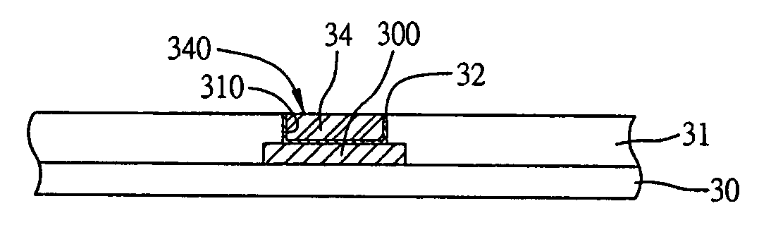
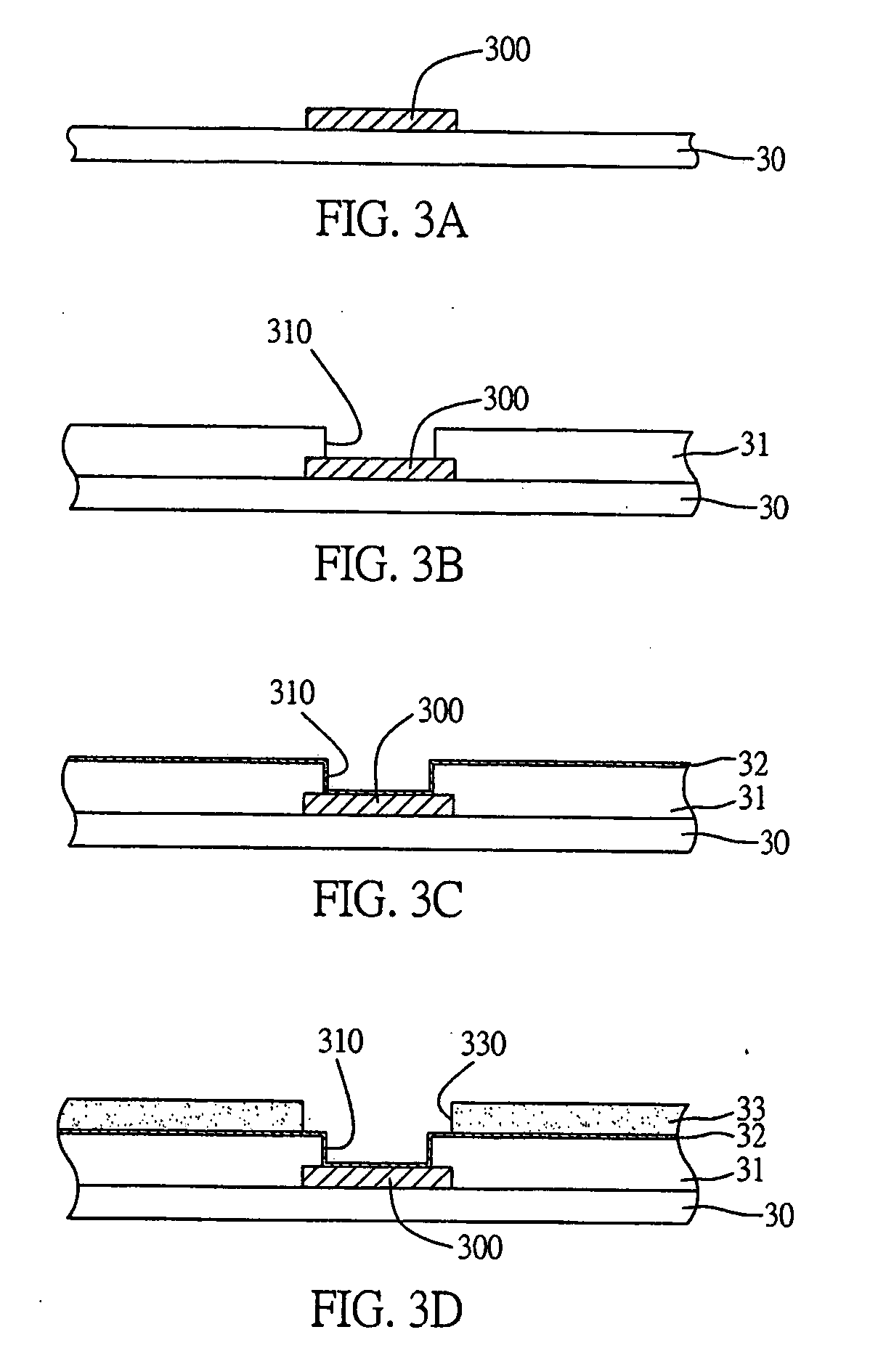
[0028]FIGS. 3A to 3G, 4A to 4B, 5 and 6 illustrate a method for fabricating an electrically connecting structure of a circuit board of a first embodiment according to the present invention.

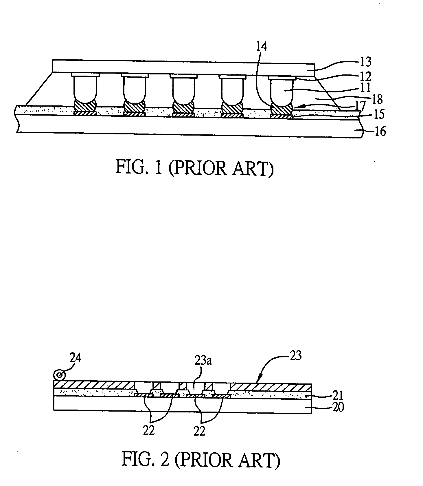
[0029] Please refer to FIG. 3A. A plurality of electrically connecting pads 300 and a conductive line (not shown) are formed on a circuit board 30, which has a layout already. Manufacturing techniques for forming the conductive line and the electrically conn...


PUM


Abstract

A method for fabricating an electrically connecting structure of a circuit board is proposed. An insulating protecting layer is formed on a circuit board having electrically connecting pads and has openings to expose the electrically connecting pads. A resist layer with openings corresponding to the electrically connecting pads is formed on a conductive layer formed on the insulating protecting layer. A metal layer is formed in the openings of the resist layer and fills the openings. The resist layer is removed. The metal layer and the conductive layer on the surface of the insulating protecting layer are removed by thinning processing, so as to form a metal bump. An adhesive layer is formed on an exposed surface of the metal bump, so as to form the electrically connecting structure for electrically connecting the circuit board to an external electronic device.

Description

CROSS-REFERENCE TO RELATED APPLICATION [0001] This application claims benefit under 35 USC 119 of Taiwan Application No. 094114845, filed May 9, 2005. FIELD OF THE INVENTION [0002] This invention relates to a method for fabricating an electrically connecting structure of a circuit board, and more particularly, to a method for fabricating an electrically connecting structure formed on electrically connecting pads of the circuit board for electrically connecting the circuit board to an external electronic device. BACKGROUND OF THE INVENTION [0003] A flip chip package technique was introduced to the market by International Business Machine (IBM) Co. in early 1960's. Compared with a wire bond technique, the flip chip package technique has a characteristic that a semiconductor chip is electrically connected to a substrate by solder bumps, rather than by gold wires. A semiconductor component made by the flip chip package technique has a smaller size and a larger density. Moreover, because...

Claims


Application Information

Patent Timeline
IPC IPC(8): H01L21/44
CPCH05K3/045H05K3/243H05K3/28H05K2203/0723H05K2201/0367H05K2203/0353H05K2203/054H05K3/4007
Inventor HU, WEN-HUNG
Owner PHOENIX PRECISION TECH CORP
Why Eureka
Try Eureka