

Semiconductor device
a semiconductor and semiconductor technology, applied in the direction of semiconductor devices, electrical equipment, transistors, etc., can solve the problems of increasing achieve the effects of reducing the area of the device, reducing the drain, and reducing the distance between the isolation trench and the source region
- Summary
- Abstract
- Description
- Claims
- Application Information
AI Technical Summary
Benefits of technology
Problems solved by technology
Method used
Image

Examples
Embodiment Construction
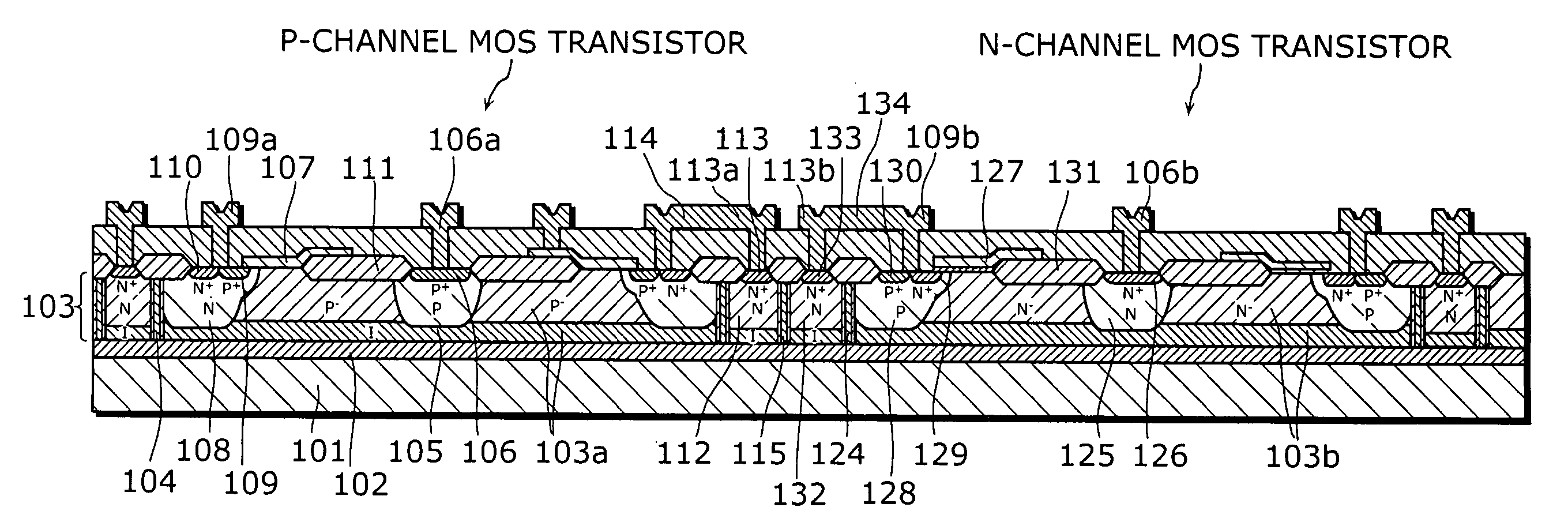
[0042] Hereafter, a semiconductor device of an embodiment for the present invention will be described referring to the drawings. However the present invention is not limited merely to the embodiment mentioned below.
[0043] The semiconductor device of the embodiment includes a P-channel MOS transistor and an N-channel MOS transistor adjacent to the P-channel MOS transistor.
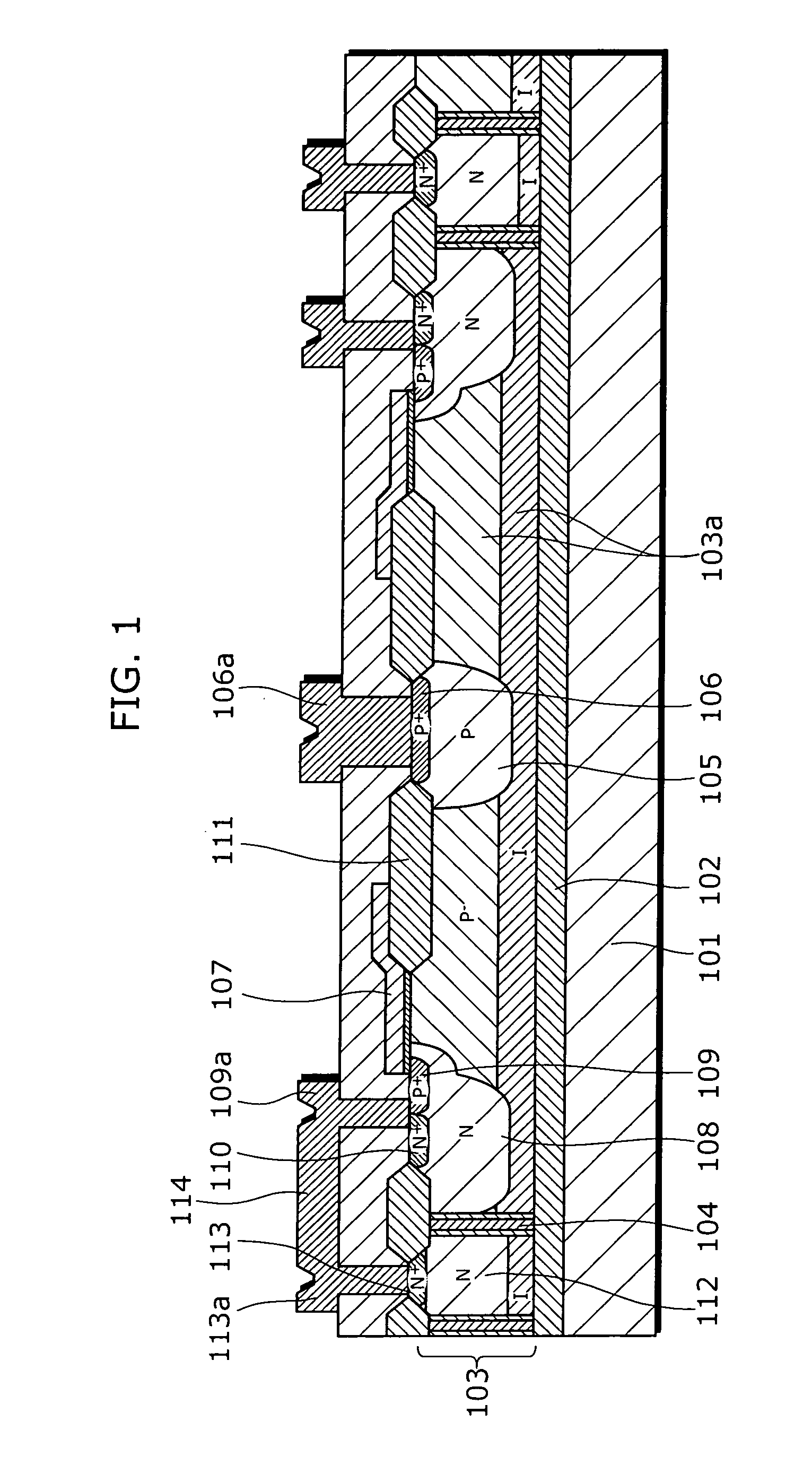
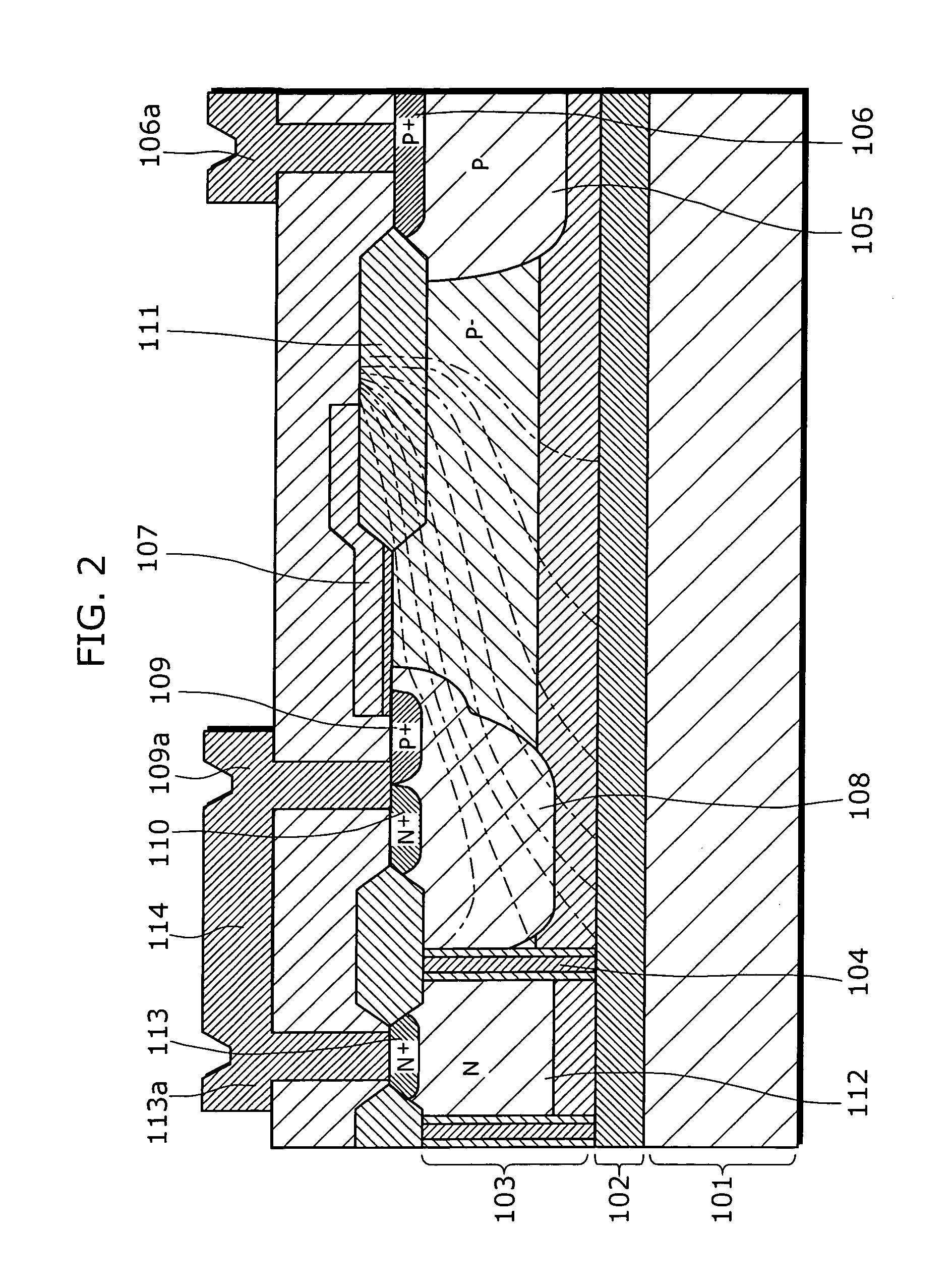
[0044]FIG. 5 is a cross sectional diagram of the P-channel MOS transistor structuring a semiconductor device according to the embodiment for the present invention.
[0045] As shown in FIG. 5, the P-channel MOS transistor includes an SOI substrate which has a semiconductor substrate 1, a buried oxide film 2 of 1 to 3 μm in thickness placed on the semiconductor substrate 1, and a P-type semiconductor layer 3 of 3 to 5 μm in thickness placed on the buried oxide film 2. An island-like semiconductor layer 3a, in which the P-channel MOS transistor structure is formed, isolated from other portions of the semiconductor lay...
PUM
 Abstract
Description
Claims
Application Information