

Semiconductor substrate, field-effect transistor, and their production methods
- Summary
- Abstract
- Description
- Claims
- Application Information
AI Technical Summary
Benefits of technology
Problems solved by technology
Method used
Image

Examples
examples
[0197] Next, worsening of the roughness at the surface and interfaces when heat treatment is performed prior to polishing based on the above embodiments is explained in detail, referring to FIG. 18 and FIG. 19.
[0198] As an example based on the above seventh embodiment and a comparative example, films were deposited, in both cases using a Si substrate of diameter 200 mm, with a single-wafer reduced-pressure epitaxial growth system employed to deposit films with SiH4 and GeH4 intermixed with the carrier hydrogen gas, at pressures between 5000 and 15,000 Pa and temperatures of 680 to 850° C. FIG. 18 is a flow chart of fabrication of the example and comparative example.
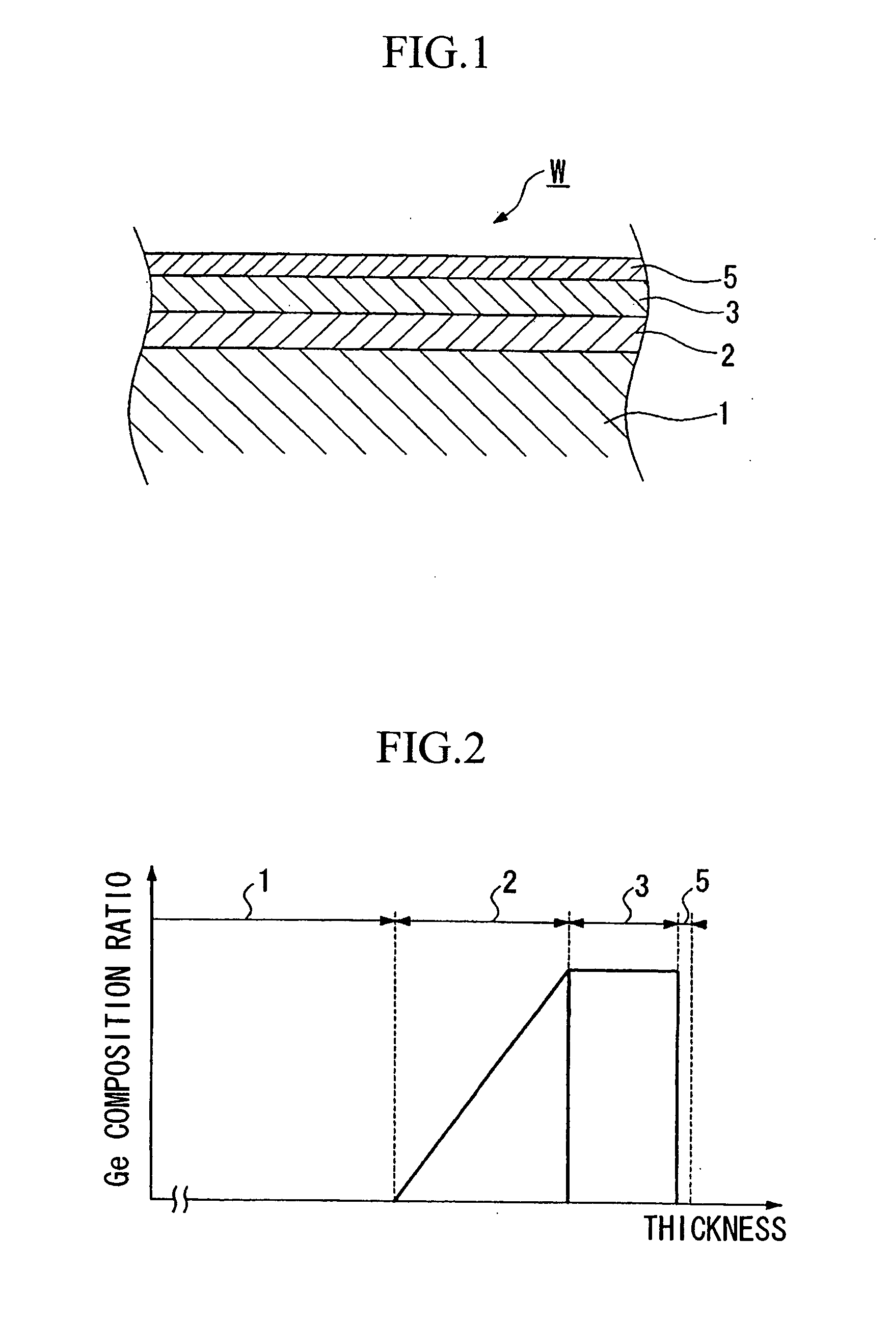
[0199] In this case, prior to annealing treatment and polishing, the first SiGe layer 2, second SiGe layer 3, relaxation layer 4, and strained Si layer 5 were deposited to respective thicknesses of 30 nm, 2.0 μm, 1.0 μm, and 20 nm, as indicated in FIG. 19. The Ge composition ratio of the first SiGe layer 2 was 0. 15, an...
PUM
 Abstract
Description
Claims
Application Information