Metal-induced crystallization of amorphous silicon, polycrystalline silicon thin films produced thereby and thin film transistors produced therefrom

a technology of amorphous silicon and crystallization, which is applied in the direction of semiconductor devices, electrical appliances, basic electric elements, etc., can solve the problems of increasing the cost of doing so, difficult to realize peripheral circuits, and low operating speed, so as to reduce the amount of residual metal elements and improve the quality of the resulting polycrystalline silicon

Active Publication Date: 2006-11-23
THE HONG KONG UNIV OF SCI & TECH
View PDF23 Cites 35 Cited by
  • Summary
  • Abstract
  • Description
  • Claims
  • Application Information

AI Technical Summary

Benefits of technology

[0016] The present invention allows the introduction of a sufficient amount of metal elements to nucleate MIC, while providing a technique for removing some of the metal elements during the subsequent crystallization heat treatment. Consequently, the quality of the resulting polycrystalline silicon is improved and the amount of residual metal elements is reduced.

Problems solved by technology

TFTs based on amorphous silicon suffer from low operating speed and lack of a p-type device, making it difficult to realize peripheral circuits.
The traditional approach of increasing device density is to improve micro-lithography resolution, the cost of doing which is becoming increasingly prohibitive.
Polycrystalline silicon obtained by conventional low-pressure chemical vapor deposition suffers from relatively high process temperatures (620-650° C.) and poor material quality.
However, this is only possible for much more expensive quartz substrates but not for inexpensive glass substrates.
Such metal residual is considered a contaminant and degrades the performance of the devices on the resulting polycrystalline silicon thin film.
This is undesirable for very thin films of polycrystalline silicon.
The presence of the bottom gettering layer and nickel gettered into it may affect the material quality and the characteristics of the devices built on the resulting polycrystalline silicon.

Method used


Image

  • Metal-induced crystallization of amorphous silicon, polycrystalline silicon thin films produced thereby and thin film transistors produced therefrom
  • Metal-induced crystallization of amorphous silicon, polycrystalline silicon thin films produced thereby and thin film transistors produced therefrom
  • Metal-induced crystallization of amorphous silicon, polycrystalline silicon thin films produced thereby and thin film transistors produced therefrom

Examples


Embodiment Construction

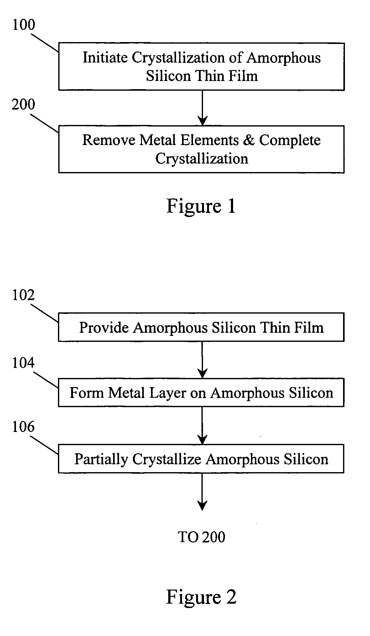
[0035]FIG. 1 is a flowchart indicating the basic steps of a process which embodies a first exemplary embodiment of the invention. In step 100, crystallization of an amorphous silicon thin film is initiated to provide a partially crystallized amorphous silicon thin film. In step 200, metal elements in the partially crystallized amorphous silicon thin film are removed and the crystallization of the amorphous silicon thin film is completed (to the extent required).

[0036]FIG. 2 is a flowchart indicating an exemplary set of component steps in the initiating step 100 of FIG. 1. The amorphous silicon thin film is first provided, in step 102. It may be pre-formed prior to the present process or formed as an initial part of the present process in any known way. For example it may be formed at a low temperature, between about 150° C. to about 600° C., using any of a variety of techniques including but not limited to sputtering, evaporation, low-pressure thermal or plasma-enhanced chemical va...


PUM

PropertyMeasurementUnit
temperatureaaaaaaaaaa
thickaaaaaaaaaa

Abstract

Crystallization-inducing metal elements are introduced onto an amorphous silicon thin film. A first, low-temperature, heat-treatment induces nucleation of metal-induced crystallization (MIC), resulting in the formation of small polycrystalline silicon “islands”. A metal-gettering layer is formed on the resulting partially crystallized thin film. A second, low-temperature, heat-treatment completes the MIC process, whilst gettering metal elements from the partially crystallized thin film. The process results in the desired polycrystalline silicon thin film.

Description

CROSS-REFERENCE TO RELATED APPLICATIONS [0001] This application claims priority under 35 U.S.C. §119 to U.S. Provisional Application No. 60 / 675,300, filed Apr. 28, 2005, which is herein incorporated by reference in its entirety.FIELD OF THE INVENTION [0002] The present invention relates to the crystallization of amorphous silicon, in particular by way of metal-induced crystallization, polycrystalline silicon thin films produced thereby and thin film transistors produced therefrom. BACKGROUND OF THE INVENTION [0003] Thin film transistors (TFTs) are used in the construction of active-matrix liquid-crystal displays, active-matrix organic light emitting diode displays, active-matrix e-ink electronic books and active-matrix image sensors. TFTs based on amorphous silicon suffer from low operating speed and lack of a p-type device, making it difficult to realize peripheral circuits. There is a drive to switch to polycrystalline silicon devices obtained from amorphous silicon. [0004] Furthe...

Claims


Application Information

Patent Timeline
Patent Type & Authority Applications(United States)
IPC IPC(8): H01L21/84
CPCH01L21/02532H01L21/02667H01L21/02672H01L29/78675H01L27/1296H01L29/04H01L27/1277
Inventor WONG, MANKWOK, HOI-SINGMENG, ZHIGUOZHANG, DONGLISHI, XUEJIE
Owner THE HONG KONG UNIV OF SCI & TECH
Why Eureka
Try Eureka