Integrated circuit (IC) with on-chip programmable fuses

a programmable fuse and integrated circuit technology, applied in the field of forming fuses, can solve the problems of difficult control of window thickness, difficult to control the thickness of the window, and the entire array of chips may not be able to test well, so as to eliminate or reduce the damage of ic chips at programmed fuses and eliminate or reduce ic chip loss at fuse programming

Inactive Publication Date: 2006-11-30
IBM CORP
View PDF13 Cites 10 Cited by
  • Summary
  • Abstract
  • Description
  • Claims
  • Application Information

AI Technical Summary

Benefits of technology

[0009] It is a purpose of the invention to improve IC chip yield;
[0010] It is another purpose of the invention to eliminate or reduce IC chip damage at programmed fuses;
[0011] It is another purpose of the invention to eliminate or reduce IC chip loss at fuse programming;

Problems solved by technology

A defect in just one cell could ruin the entire array.
During initial chip test, some chip arrays may have rows and / or columns that test bad.
Unfortunately, especially with upper dielectric layers made of softer, mechanically weaker low-k dielectric, all of the programming energy collecting in the fuse does not necessarily escape through the window and, instead, is directed downward and laterally.
Since it is difficult to control window thickness, in some instances blowing the fuse fractures the chip dielectric encasing the fuse and cracks adjacent and underlying low-k dielectric layers.
At worst, these cracks may radiate through underlying wiring, causing opens and shorts in the chip wiring, i.e., introducing defects or failures into previously good chip areas.
These cracks may expose underlying, formerly protected and passivated circuitry to contamination, e.g., moisture.
The moisture may reduce chip reliability and, ultimately cause the damaged chip to fail.
This may be much harder to diagnose and may not manifest itself until the chip is already in use in the field.
Consequently, for these chips the cure may be worse than the defect and blowing fuses to recover failing chips may destroy the chips, turning partially good chips to all bad or suspect, frustrating the purpose of including the fuses in the first place.

Method used


Image

  • Integrated circuit (IC) with on-chip programmable fuses
  • Integrated circuit (IC) with on-chip programmable fuses
  • Integrated circuit (IC) with on-chip programmable fuses

Examples


Embodiment Construction

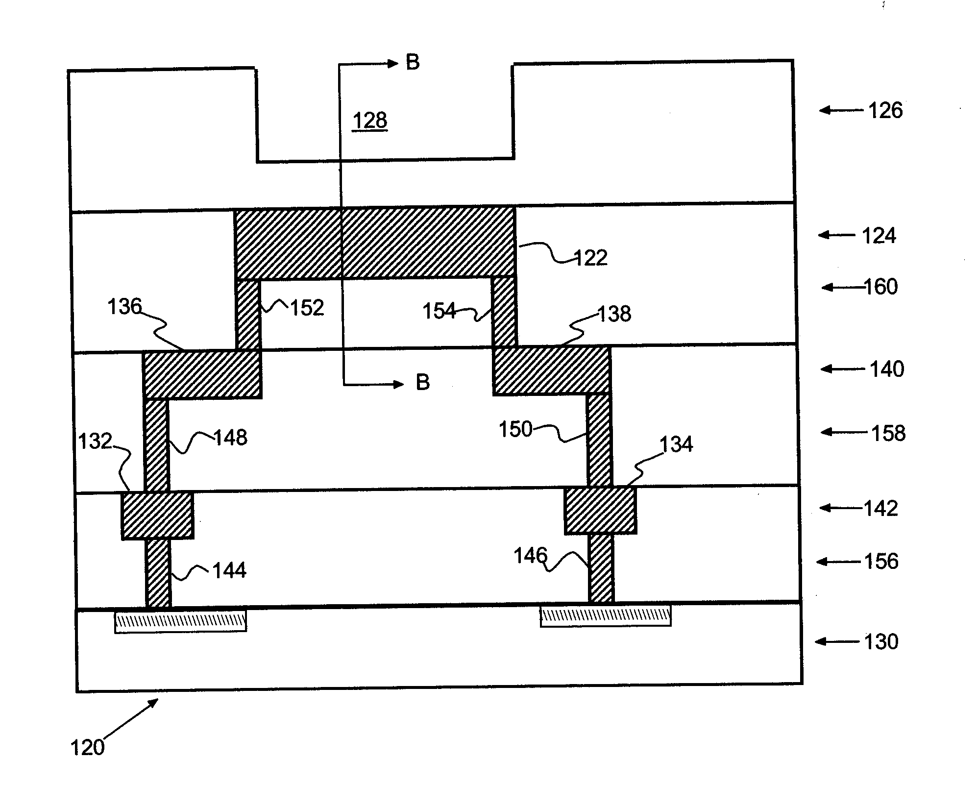
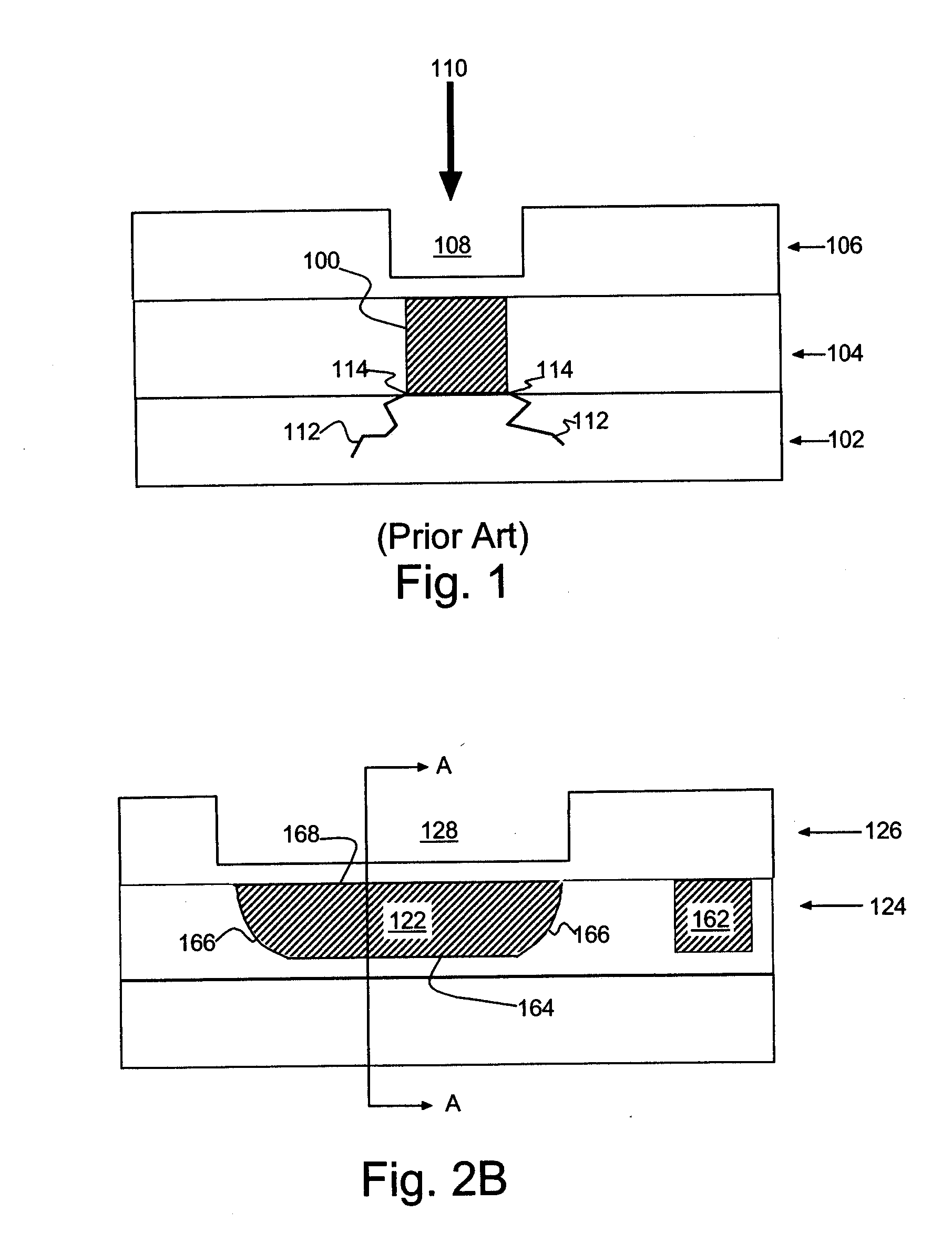
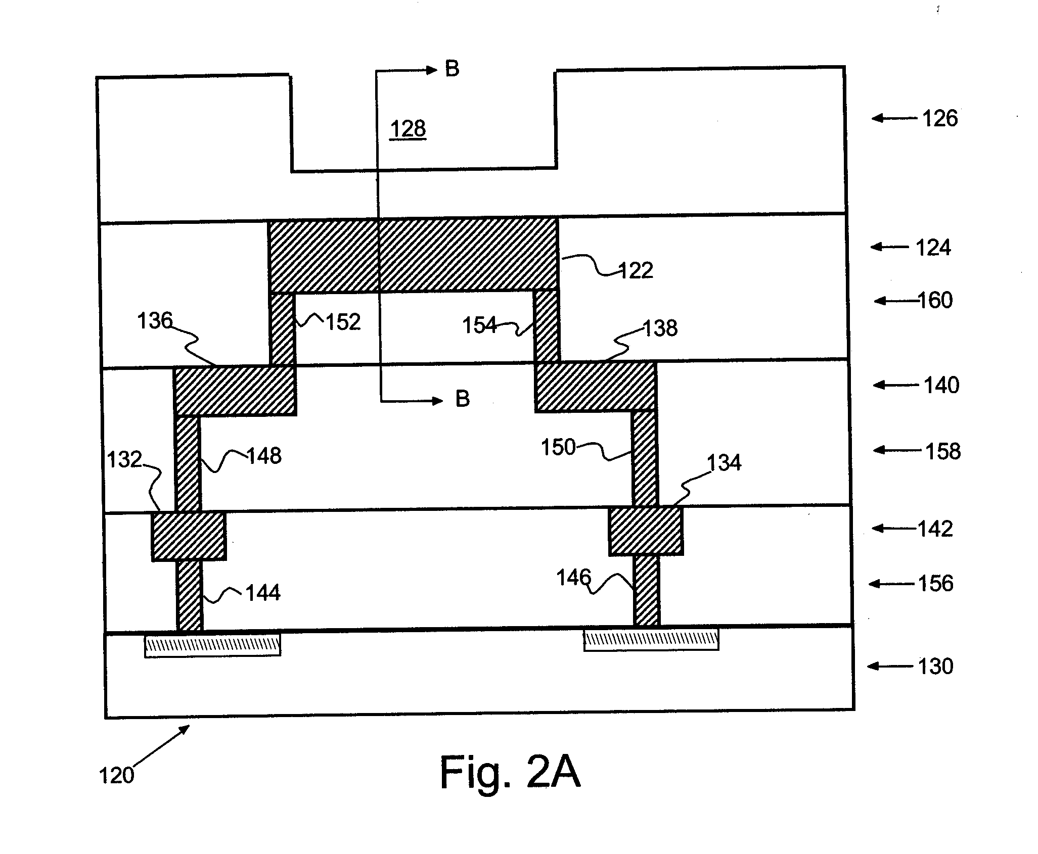
[0019] Turning now to the drawings and, more particularly, FIG. 1 shows the effect on surrounding structures of blowing a prior art fuse 100 encased in a dielectric layers 102, 104 and passivation layer 106 (e.g., separating wiring or terminal metallurgy layers) with a thinned dielectric window 108 formed in dielectric layer 106 above the fuse 100. Low-k dielectric materials in the dielectric layers 102, 104 are softer and mechanically weaker than the typical material in the passivation layer 106. So, when energy (e.g., laser energy 110) is applied to the fuse 100, as the fuse material heats and expands some damage 112 is inflicted on the low-k dielectric layers 102, 104 at least until the material fractures the window 108 and escapes through the open window. The severity of the damage varies depending upon any number of factors, e.g., window thickness, fuse thickness and depth, energy source and level and etc. Because etching the passivation layer 106 is imprecise, it is very diffi...


PUM


Abstract

An Integrated Circuit (IC) chip with fused circuits and method of making the IC. Fuses in an upper wiring layer are formed using a multi-tone mask to define rounded bottom corners on the fuses, while wiring in the upper wiring layer maintain a rectangular cross-section.

Description

BACKGROUND OF THE INVENTION [0001] 1. Field of the Invention [0002] The present invention is related to Integrated Circuit (IC) chip manufacture and more particularly to forming fuses on IC chips. [0003] 2. Background Description [0004] Fuses on Integrated Circuit (IC) chips are well known in the art and are commonly included in IC chips with arrays of identical elements, repetitious identical circuits or even for late (in the manufacturing process) programming, e.g., selectively blowing fuses to set chip select addresses. A Random Access Memory (RAM), for example, includes an array of identical RAM cells. A defect in just one cell could ruin the entire array. So, typically IC chips with such arrays or even numerous identical copies of the same circuit, are designed with extra, identical, replacement copies or spares units, i.e., of array elements or selected chip circuits. When a bad or defective unit is identified, e.g., through chip test, the bad unit may be swapped, electrically...

Claims


Application Information

Patent Timeline
Patent Type & Authority Applications(United States)
IPC IPC(8): H01L29/00
CPCH01L23/5258H01L2924/0002H01L2924/00
Inventor DAUBENSPECK, TIMOTHY H.GAMBINO, JEFFREY P.MUZZY, CHRISTOPHER D.SAUTER, WOLFGANG
Owner IBM CORP
Why Eureka
Try Eureka