

Computing method for meal gate surface appearance
A technology of surface topography and calculation method, applied in computing, instrumentation, electrical and digital data processing, etc., can solve problems affecting surface topography, metal dishing and dielectric erosion, and inability of integrated circuit chips to work, and improve chip quality. rate effect
- Summary
- Abstract
- Description
- Claims
- Application Information
AI Technical Summary
Problems solved by technology
Method used
Image

Examples
Embodiment Construction
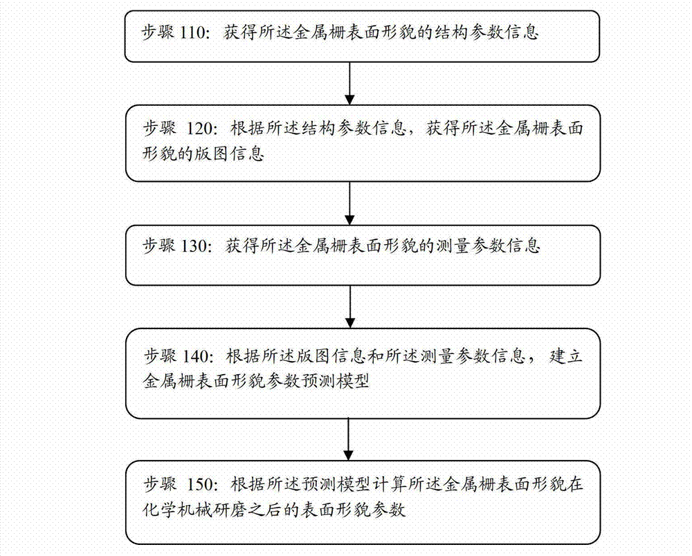
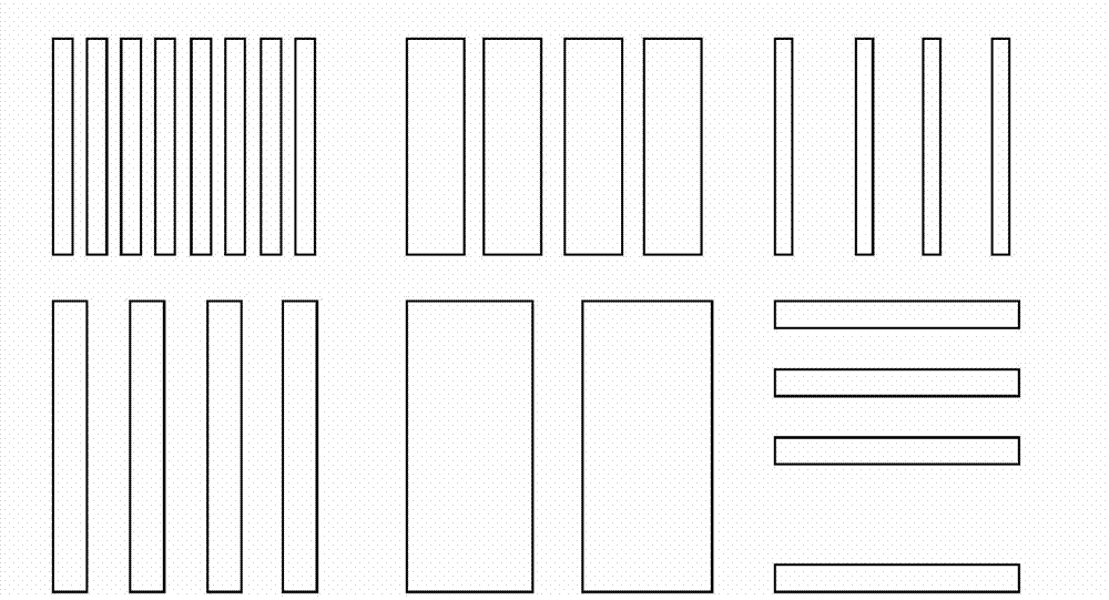
[0017] In the embodiments of the present invention, by obtaining the layout information and measurement parameter information of the surface topography of the metal gate, a prediction model of the surface topography parameters of the metal gate is established. Through the prediction model, the surface of the designed metal gate structure after CMP can be analyzed in the chip design process. Predict the shape of the metal grid to obtain the dishing shape of the metal grid and the erosion shape of the dielectric between the metal grids, so as to find out the areas that may have problems after the CMP process step in the design, such as the excessive value of the metal grid dishing Large and other areas are provided for designers to improve, thereby avoiding corresponding problems in the manufacturing process, thereby improving the yield rate of products.
[0018] Such as figure 1 As shown, the embodiment of the present invention provides a method for calculating the surface topo...
PUM
 Abstract
Description
Claims
Application Information