Semiconductor device
- Summary
- Abstract
- Description
- Claims
- Application Information
AI Technical Summary
Benefits of technology
Problems solved by technology
Method used
Image

Examples
embodiment mode 1
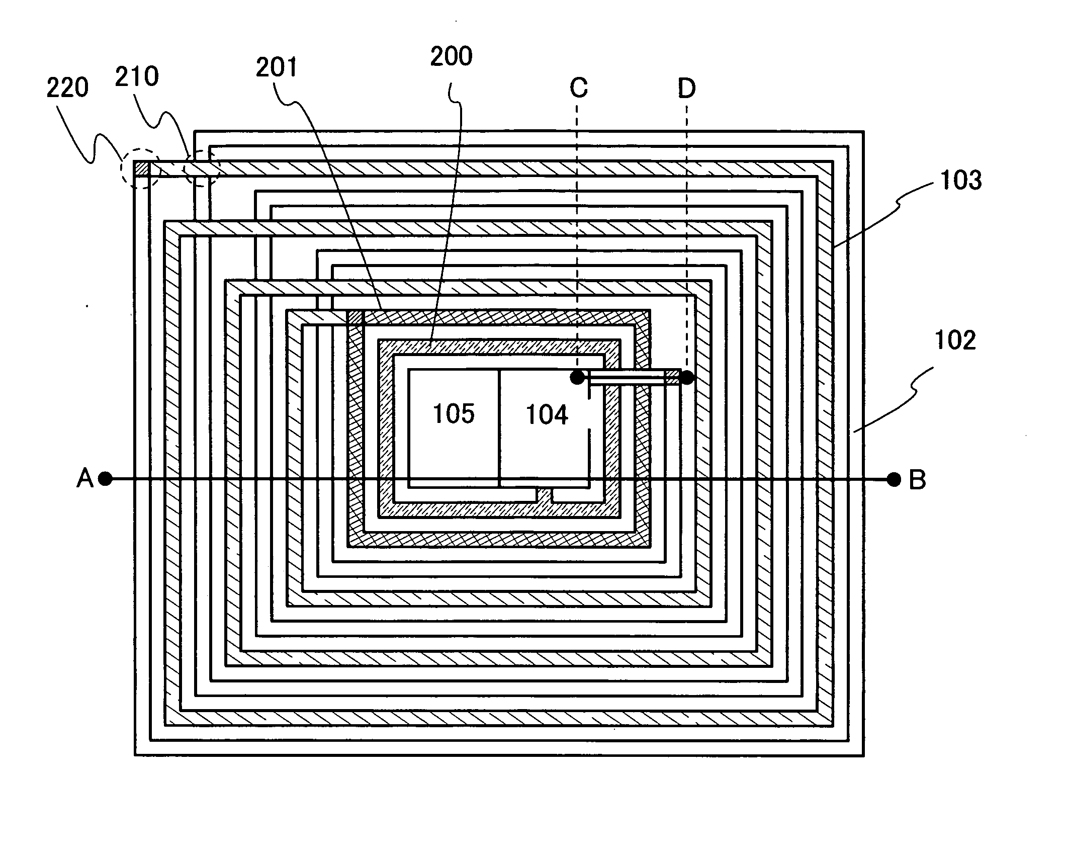
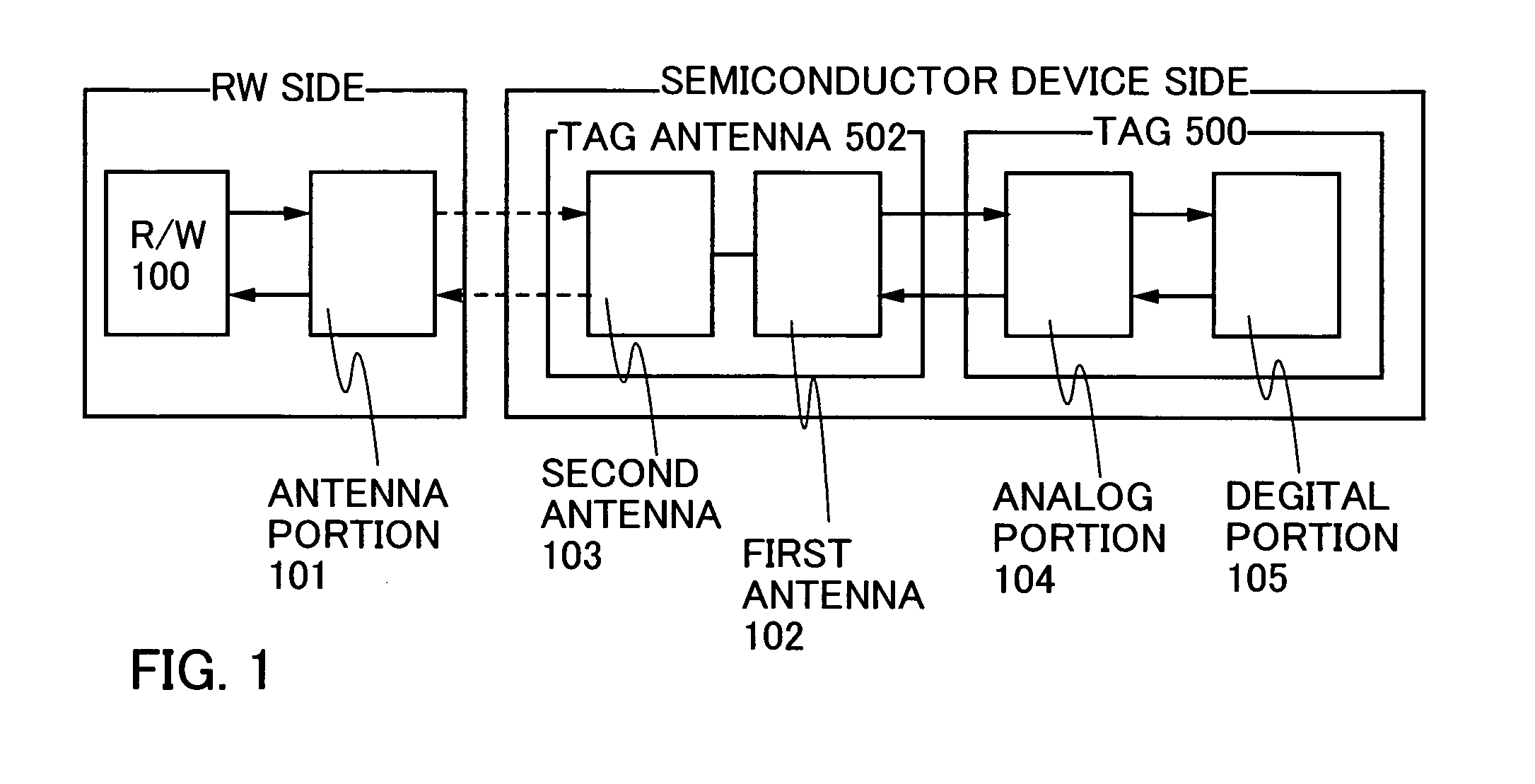
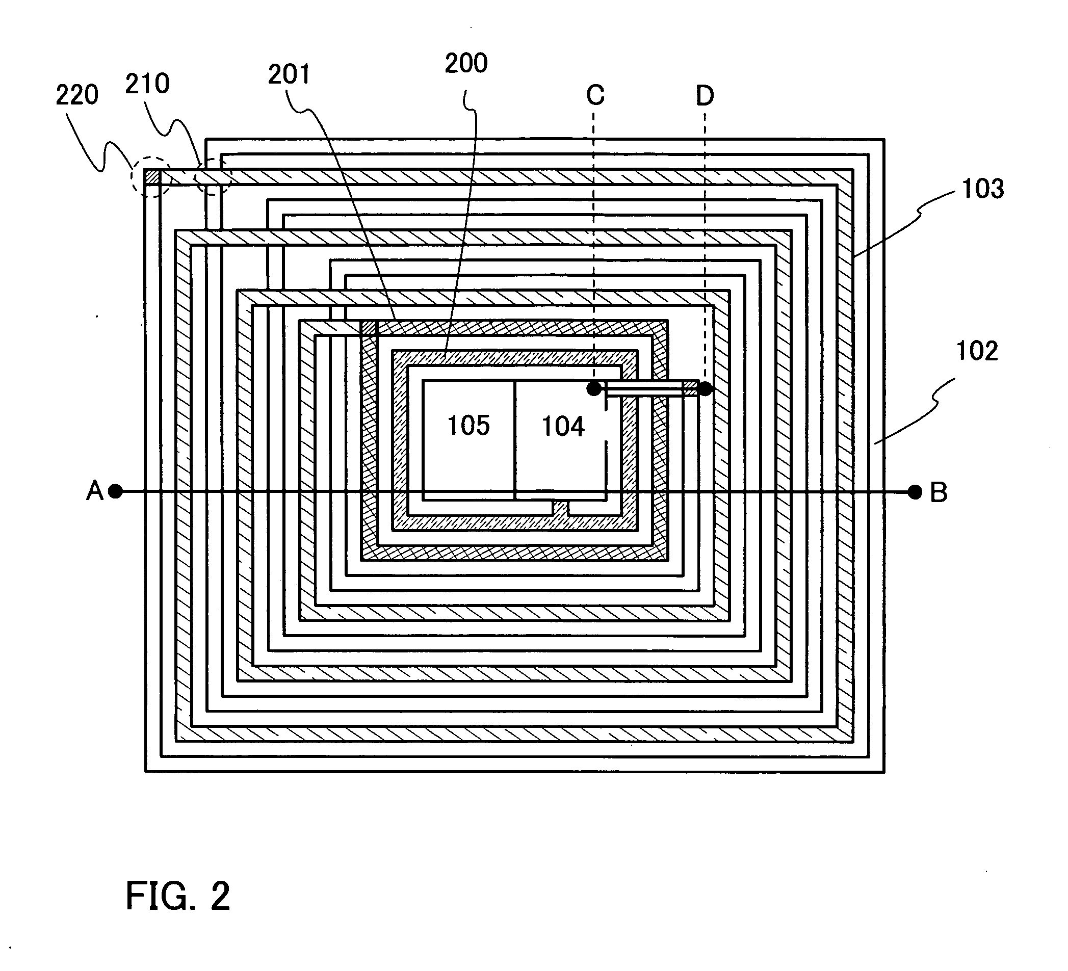
[0040] An embodiment mode of the present invention is explained with reference to drawings. FIG. 1 is a diagram showing an example of a structure of a semiconductor device that can exchange data without contact. The semiconductor device that can transmit and receive data by wireless communication is also referred to as an RFID (Radio Frequency Identification) tag, an ID tag, an IC tag, an IC chip, an RF (Radio Frequency) tag, a wireless tag, an electronic tag, or a wireless chip depending on its application mode. In the present invention, it is referred to as an RFID tag for convenience, but it can be applied to any of the above modes. The semiconductor device that can transmit and receive data by wireless communication communicates data and transmits and receives power between an antenna portion 101 of a read / write communication control circuit 100 (hereinafter referred to as a reader / writer or R / W) and a tag antenna 502 of the semiconductor device that can transmit and receive dat...
embodiment mode 2
[0052] A method for manufacturing the semiconductor device of the present invention that can transmit and receive data by wireless communication is explained in this embodiment mode with reference to FIGS. 10A to 10C. In this embodiment mode, a thin film element in a tag is explained, while showing only a single thin film transistor in an analog portion. Note that another thin film element can also be manufactured in a similar manner, and it is easy for a person skilled in the art to apply this manufacturing method to another thin film element based on common general technical knowledge.
[0053] As the substrate 300, a glass substrate of barium borosilicate glass, alumino borosilicate glass, or the like, a quartz substrate, a ceramic substrate, or the like can be used. In addition, a semiconductor substrate on a surface of which an insulating film is formed may be used. A flexible substrate such as a plastic substrate may be used. Further, the surface of the substrate may be polished...
embodiment 1
[0075] In this embodiment, applications of the semiconductor device of the present invention are explained with reference to FIGS. 11A and 11B, FIGS. 12A to 12E and FIGS. 18A and 18B. A semiconductor device 700 of the present invention can be mounted on, for example, paper money, coins, securities, bearer bonds, a certificate (such as a driver's license or a resident's card (see FIG. 12A)), a packing case (such as a wrapper or a bottle (see FIG. 12B)), a recoding medium such as DVD software, a CD, or a video tape (see FIG. 12C), a vehicle such as a car, a motorcycle, or a bicycle (see FIG. 12D), personal belongings such as a bag or glasses (see FIG. 12E), food, clothing, commodities, an electronic device, or the like. The electronic device includes a liquid crystal display device, an EL display device, a television device (also simply referred to as TV or a television receiver), a cellular phone, and the like.
[0076] The semiconductor device of the invention can be fixed to an artic...
PUM
 Abstract
Description
Claims
Application Information
 - R&D
- Intellectual Property
- Life Sciences
- Materials
- Tech Scout
- Unparalleled Data Quality
- Higher Quality Content
- 60% Fewer Hallucinations
Browse by: Latest US Patents, China's latest patents, Technical Efficacy Thesaurus, Application Domain, Technology Topic, Popular Technical Reports.
© 2025 PatSnap. All rights reserved.Legal|Privacy policy|Modern Slavery Act Transparency Statement|Sitemap|About US| Contact US: help@patsnap.com