Memory module with improved mechanical strength of chips

Active Publication Date: 2006-11-30
MICRON TECH INC
View PDF5 Cites 61 Cited by
  • Summary
  • Abstract
  • Description
  • Claims
  • Application Information

AI Technical Summary

Benefits of technology

[0007] It is an object of the present invention to provide a memory module in which the

Problems solved by technology

In the techniques disclosed in the foregoing documents, the lowermost chip is in danger of breakage beca

Method used


Image

  • Memory module with improved mechanical strength of chips
  • Memory module with improved mechanical strength of chips
  • Memory module with improved mechanical strength of chips

Examples


Embodiment Construction

[0021] A memory module of the present invention is characterized in that a heat dissipating plate is provided in proximity to an interface chip for dissipating heat generated by the operating memory module, and a substrate, which underlies an interposer chip, is made of a semiconductor material that is similar to a memory core chip in order to restrain thermal strains and distortions due to heat.

[0022] A method of manufacturing a memory module in turn is characterized in that the heat dissipating plate serves as a support for increasing the mechanical strength of the chips. The method is also characterized by manufacturing a plurality of memory modules based on a single support.

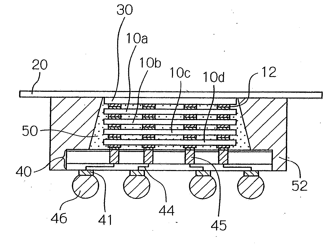
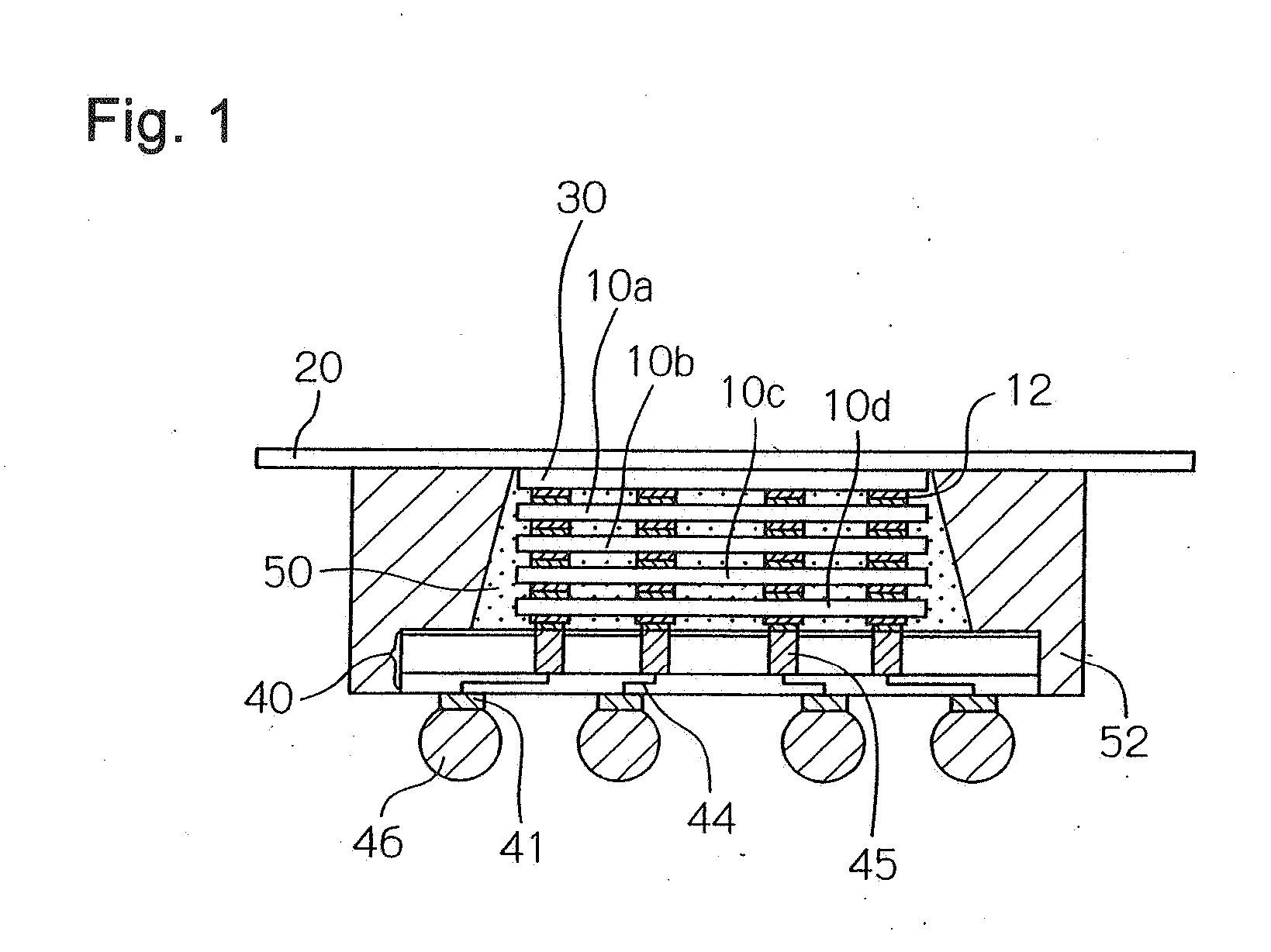
[0023] In one embodiment, laminated memories are DRAM's (Dynamic Random Access Memory). FIG. 1 is a schematic cross-sectional view illustrating an exemplary configuration of a memory module according to this embodiment.

[0024] As illustrated in FIG. 1, the memory module of this embodiment comprises memory c...


PUM


Abstract

A memory module of the present invention has a memory core chip for storing information, an interface chip for controlling data input/output, an interposer chip for transmitting/receiving data to/from the outside, and an external connection terminal provided in closest proximity to the interposer chip. A heat dissipating plate is provided in closest proximity to the interface chip. The interposer chip has a substrate made of a semiconductor material that is similar to the memory core chip, a land for holding the external connection terminal, a wire connected to the external connection terminal, and an insulating film for insulating the wire. The land, wire, and insulating film are integrally formed on one surface of the interposer chip.

Description

BACKGROUND OF THE INVENTION [0001] 1. Field of the Invention [0002] The present invention relates to a memory module having a semiconductor memory chip, and a method of manufacturing the same. [0003] 2. Description of the Related Art [0004] Heretofore, JP-A-63-156348 and JP-A-2002-170919 disclose structures for laminating a plurality of LSI's (Large Scale Integrated circuit) by providing through-electrodes in semiconductor chips made of silicon or the like which are formed with circuits, and methods of manufacturing such structures. In these disclosed techniques, laminated LSI's and underlying substrates are all singularized into chips, and sequentially laminated using connection electrodes provided in each of the chips to form a memory module having desired functions. [0005] In the techniques disclosed in the foregoing documents, the lowermost chip is in danger of breakage because it is repeatedly applied with force when bumps are bonded or thermo-compression bonded to each other. ...

Claims


Application Information

Patent Timeline
IPC IPC(8): H01L23/34
CPCH01L25/0657H01L25/18H01L2224/16145H01L2225/06513H01L2225/06517H01L2924/01019H01L2225/06586H01L2225/06589H01L2924/01078H01L2924/01079H01L2924/15311H01L2225/06541H01L2924/00014H01L2924/00011H01L2224/0401
Inventor ISHINO, MASAKAZUIKEDA, HIROAKI
Owner MICRON TECH INC
Why Eureka
Try Eureka