Integrated circuit device

a circuit device and integrated circuit technology, applied in the direction of generating/distributing signals, pulse techniques, instruments, etc., can solve the problems of delay caused by external load, not taken into account, and many digital noise, so as to achieve less digital noise, reduce the effect of external load, and increase the stable area

Inactive Publication Date: 2006-11-30
PANASONIC CORP
View PDF2 Cites 0 Cited by
  • Summary
  • Abstract
  • Description
  • Claims
  • Application Information

AI Technical Summary

Benefits of technology

[0037] According to the present invention, the power fluctuation area of the output terminal and the power fluctuation area of the logic circuit are overlaid on each other, so that a stable area having less digital noise can be increased. Therefore a camera system using the integrated circuit device of the present invention makes it possible to adjust the timing of analog processing and easily perform analog processing in the stable area having less digital noise, so that the influence of digital noise is minimized and the best picture quality can be stably obtained.
[0038] The present invention makes it possible to easily achieve analog processing in a stable area less susceptible to the influence of digital noise even in a small camera system having a large number of pixels. Further, the stable area and the adjustment range become larger and thus the picture quality can be easily adjusted.
[0039] According to the present invention, since the stable area increases, high picture quality can be achieved and an operation margin for absorbing the influence of individual variations or the like can be obtained.

Problems solved by technology

However, in the conventional integrated circuit device for processing a camera signal, delay caused by the influence of an internal layout (elements placed between the logic circuit and the output terminals and the wire lengths of the elements) and an external load has not been taken into consideration.
In the integrated circuit device, much digital noise occurs when the processing of the digital signal changes.
In the presence of a phase difference between the internal reference clock and the external output clock and between the internal data and the external output data, the area of digital noise increases.
In a camera system, such digital noise acts as a noise source to an analog signal in an image sensor and an analog processing circuit, so that an S / N ratio decreases and picture quality degrades.
However, as the operating frequency becomes faster, the stable area having less digital noise decreases and it becomes difficult to adjust the timing of analog processing to stably acquire the best picture quality.
However, when shifting the timing of outputting (phase) an external output clock and external output data including a video signal, it becomes difficult in the processing of the following stage to design the timing of receiving data by using the external output clock from an integrated circuit device.

Method used


Image

  • Integrated circuit device
  • Integrated circuit device
  • Integrated circuit device

Examples


Embodiment Construction

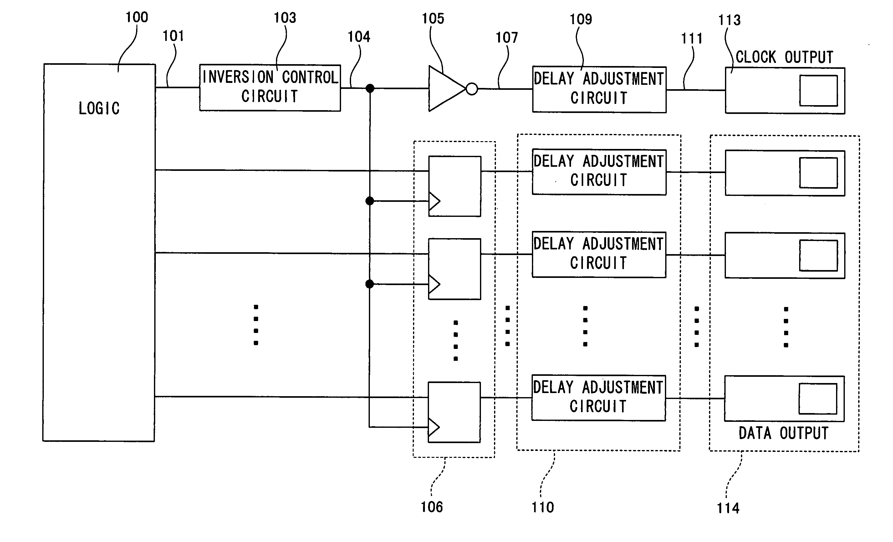
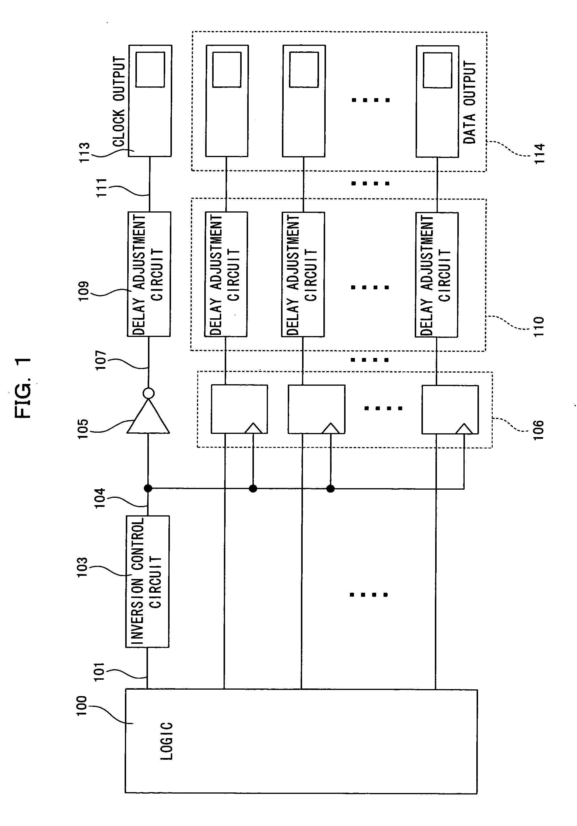
[0049] With reference to the accompanying drawings, the following will describe an integrated circuit device for processing a camera signal according to an embodiment of the present invention.

[0050]FIG. 1 is a schematic structural diagram showing a part of the integrated circuit device for processing a camera signal according to the present embodiment. The configuration of a camera system including the integrated circuit device is identical to, for example, that of FIG. 9. In the integrated circuit device, an analog processing circuit (not shown) such as an AFE is provided in the previous stage of a logic circuit.

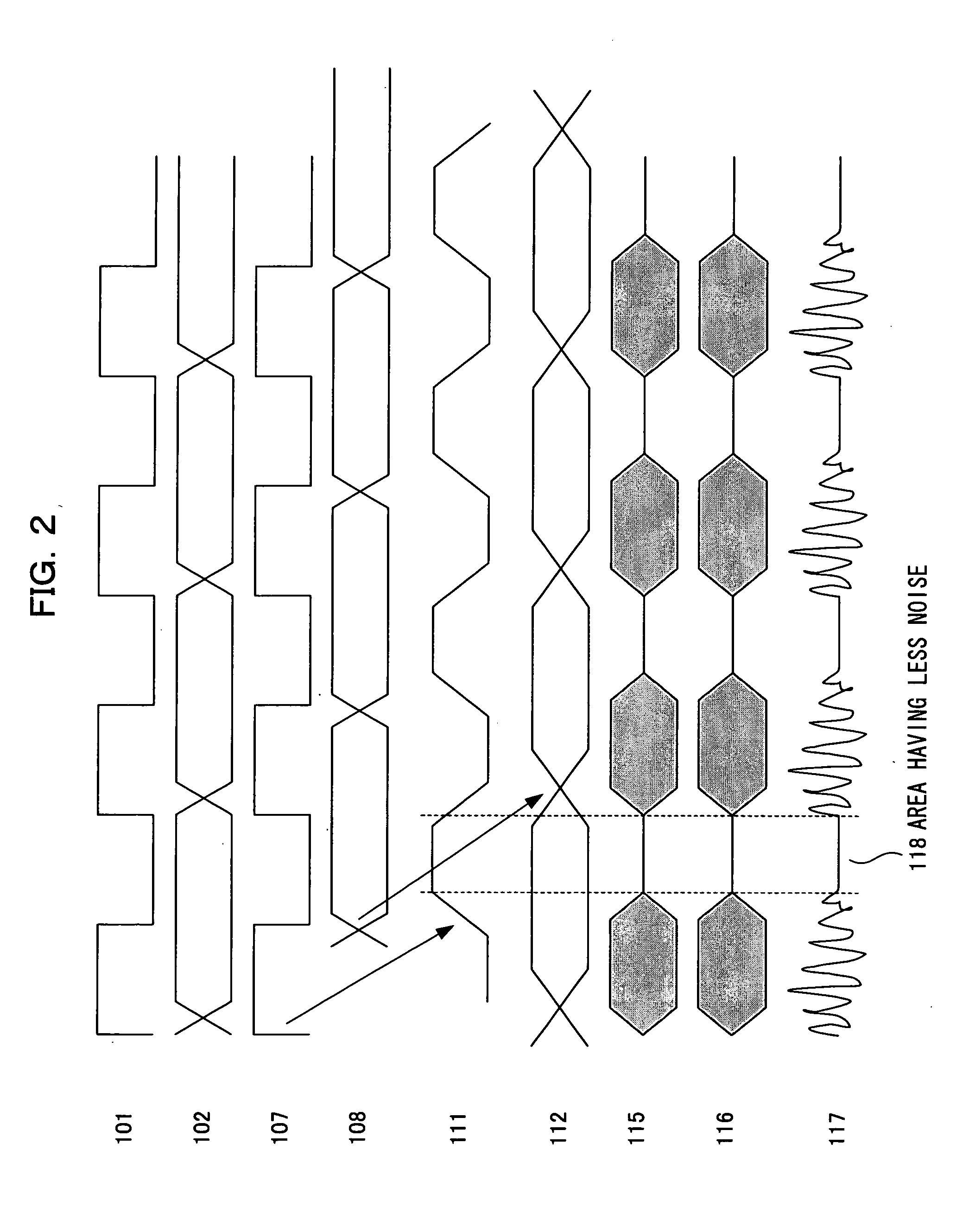
[0051]FIG. 2 is a diagram showing a timing chart for explaining the operations of the integrated circuit device for processing a camera signal according to the present embodiment. However, in the timing chart of FIG. 2, delay caused by the influence of an internal layout (elements placed between the logic circuit and output terminals and the wire lengths of the elements) ...


PUM


Abstract

An integrated circuit device is provided which can increase a stable area having less digital noise. A data delay adjustment circuit group (110) is fed with data outputted from a flip-flop circuit group (106), adjusts a delay of the data so as to synchronize the operation of a data output terminal group (114) with the operation of a logic circuit (100), and outputs the data to the data output terminal group (114). A clock delay adjustment circuit (109) similarly adjusts a delay of a clock outputted from an inverter (105) and outputs the clock to a clock output terminal (113). Therefore, the operations of data output terminals are synchronized with the operation of the logic circuit (100) while keeping the phase relationship between an external output clock and external output data.

Description

FIELD OF THE INVENTION [0001] The present invention relates to an integrated circuit device which includes at least a logic circuit serving as a synchronous circuit and outputs in parallel data generated in the logic circuit, the data being outputted with an internal reference clock used in the logic circuit. BACKGROUND OF THE INVENTION [0002] An integrated circuit device for processing a camera signal is fed with an analog signal from an image sensor or the like incorporated into a system, performs signal processing on the signal to generate a digital image signal, and outputs the signal to an image display unit incorporated into the system or an external monitor. [0003] To be specific, an integrated circuit device for processing a camera signal is first fed with an analog signal from an image sensor or the like of the previous stage, performs signal processing on the signal in an analog processing circuit such as an analog front end (AFE) or the like to convert the signal to a dig...

Claims


Application Information

Patent Timeline
Patent Type & Authority Applications(United States)
IPC IPC(8): H03H11/26
CPCH04N5/335H04N5/217H04N23/81H04N25/00
Inventor TOKUYAMA, KATSUMIHIRAYAMA, TAKESHI
Owner PANASONIC CORP
Why Eureka
Try Eureka