System and method for polymer encapsulated solder lid attach

a technology of polymer encapsulation and solder lid, which is applied in the direction of semiconductor devices, semiconductor/solid-state device details, electrical equipment, etc., can solve the problems of metal particles, inability to sufficiently transfer heat, and overheating of the integrated circuit die, so as to reduce the negative effects prevent delamination and separation, and reduce the effect of shrinkage and expansion

Inactive Publication Date: 2006-11-30
TEXAS INSTR INC
View PDF99 Cites 42 Cited by
  • Summary
  • Abstract
  • Description
  • Claims
  • Application Information

AI Technical Summary

Benefits of technology

[0012] An advantage of a preferred embodiment of the present invention is by encapsulating the metal islands in a polymer material, the different thermal characteristics of the polymer material can help to bind the metal island in place during the thermal cycles to prevent delamination and separation.
[0013] A further advantage of a preferred embodiment of the present invention is that the use of a plurality of metal islands instead of a single large monolithic sheet can help reduce the negative effects of shrinkage and expansion during a thermal cycle since the smaller dimensions of the metal islands will experience a lesser amount of shrinkage and expansion. This can further reduce the likelihood of delamination and separation.
[0014] Yet another advantage of a preferred embodiment of the present invention is that the encapsulation of the plurality of metal islands with a polymer can help to reduce the likelihood of delamination and separation since the polymer can help to bind the plurality of metal islands in place while the package experiences cool down or heat up. The binding of the plurality of metal islands can help to keep the plurality of metal islands from shifting, which could lead to delamination and separation.

Problems solved by technology

One disadvantage of the prior art is that the polymer, even with the addition of the metal particles, does not have as good a thermal conductivity as a metal material.
Therefore, in certain situations, the polymer may not be able to sufficiently transfer an adequate amount of heat.
This can lead to an overheating of the integrated circuit die, which can lead to a failure of the integrated circuit die.
A second disadvantage of the prior art is that a metal, such as solder, is relatively inflexible.
When this occurs, very little to no heat can be transferred between the integrated circuit die and the heat sink and the integrated circuit die may suffer a catastrophic failure due to overheating.

Method used


Image

  • System and method for polymer encapsulated solder lid attach
  • System and method for polymer encapsulated solder lid attach
  • System and method for polymer encapsulated solder lid attach

Examples


Embodiment Construction

[0024] The making and using of the presently preferred embodiments are discussed in detail below. It should be appreciated, however, that the present invention provides many applicable inventive concepts that can be embodied in a wide variety of specific contexts. The specific embodiments discussed are merely illustrative of specific ways to make and use the invention, and do not limit the scope of the invention.

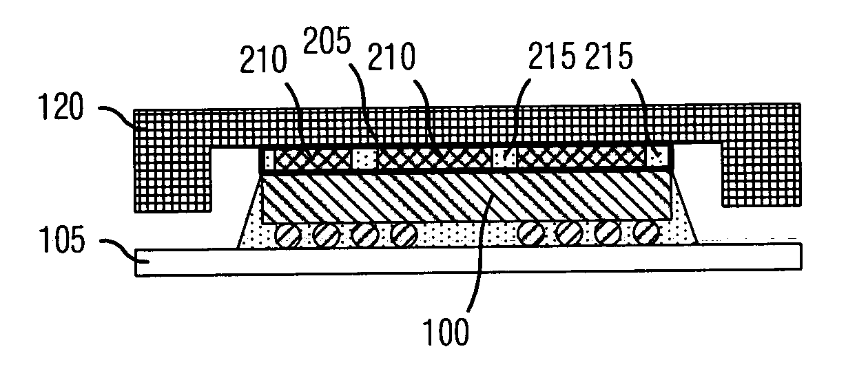
[0025] The present invention will be described with respect to preferred embodiments in a specific context, namely an attach layer for use in attaching a lid to an integrated circuit die in high-power flip-chip packages. The invention may also be applied, however, to other packaging technologies wherein an integrated circuit die is attached to a surface where thermal transfer is important and the integrated circuit die is not encapsulated by a material to lock the integrated circuit die to the surface, such as in an overmolded wirebond package at an interface between the di...


PUM

PropertyMeasurementUnit
distanceaaaaaaaaaa
metallicaaaaaaaaaa
specific temperatureaaaaaaaaaa

Abstract

System and method for a polymer encapsulated solder lid attach. A preferred embodiment comprises one or more metallic islands distributed throughout the combination attach, wherein each metallic island overlays one or more heat producing portions of the integrated circuit die, and a polymer encapsulant to encircle each metallic island and to bind the one or more metallic islands in place. The one or more metallic islands, with their high thermal conductivity, can effectively dissipate large amounts of heat, while the polymer encapsulant binds the one or more metallic islands in place, preventing (or reducing) movement occurring during thermal cycles that can lead to delamination and separation.

Description

TECHNICAL FIELD [0001] The present invention relates generally to a system and method for integrated circuits, and more particularly to a system and method for a polymer encapsulated solder lid attach. BACKGROUND [0002] Heat dissipation requires consideration when designing packaging for integrated circuits. In high performance applications, such as microprocessors, digital signal processors, controllers for high-speed communications systems, and so forth, it is not uncommon to have to dissipate hundreds of watts of power. [0003] A flip-chip package is commonly used for these high power applications. In a flip-chip package, a top surface of an integrated circuit die where the integrated circuits are actually formed is flipped over and directly attached to a substrate via solder bumps and a bottom surface of the integrated circuit die is typically attached to a lid that is attached to a heat sink. The heat generated by the integrated circuitry is primarily removed through the bottom ...

Claims


Application Information

Patent Timeline
Patent Type & Authority Applications(United States)
IPC IPC(8): H01L21/00
CPCH01L21/563H01L23/36H01L23/433H01L2224/16H01L2224/73253H01L2924/16152H01L2924/16151H01L2924/00014H01L2924/00011H01L2224/0401
Inventor CHIU, TZ-CHENGODEGARD, CHARLES ANTHONY
Owner TEXAS INSTR INC
Why Eureka
Try Eureka