System and method for automated electronic device design

a technology for electronic devices and systems, applied in the field of systems and methods for designing electronic devices, can solve the problems of complex process control problems, many design projects are not equipped to efficiently achieve the success of electronic device design, and the design of electronic devices is in effect a complex process control problem, so as to facilitate automatic selection and execution of design automation tools, the effect of facilitating expert guidan

Inactive Publication Date: 2006-11-30
PROPHICY SEMICON
View PDF10 Cites 14 Cited by
  • Summary
  • Abstract
  • Description
  • Claims
  • Application Information

AI Technical Summary

Benefits of technology

[0014] The method and system can perform abstraction of analysis results produced by the system, for a purpose of determining the root causes of design maladi

Problems solved by technology

Even though Electronic Design Automation (EDA) tools have made considerable progress in automating many of the previously manual design activities, semiconductor process technology and escalating circuit densities combine to make design an increasingly complicated and expensive undertaking.
Many design projects are ill equipped to efficiently achieve success on an electronic design project, due at least in part to the scarcity of expert designers.
Electronic device design is in effect a complex process control problem, requiring multiple passes through design tools and knowledgeable and experienced designers to control the process or flow.
Invariably intermediate results fail to meet constraints

Method used


Image

  • System and method for automated electronic device design
  • System and method for automated electronic device design
  • System and method for automated electronic device design

Examples


Embodiment Construction

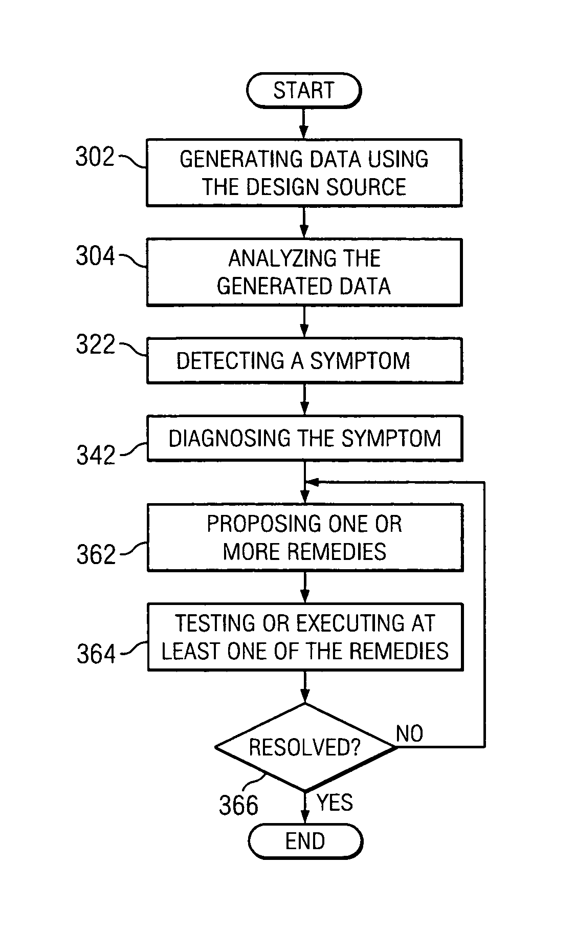
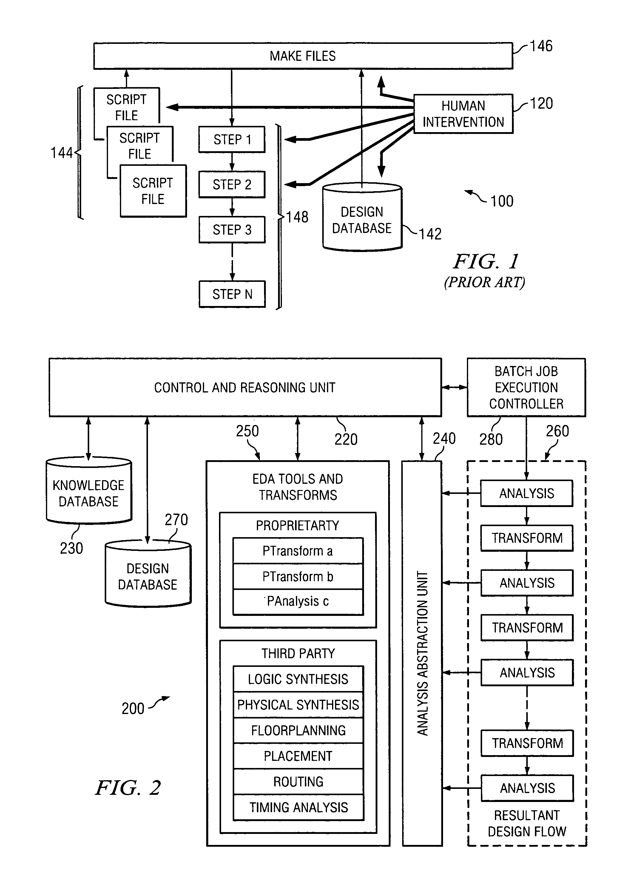
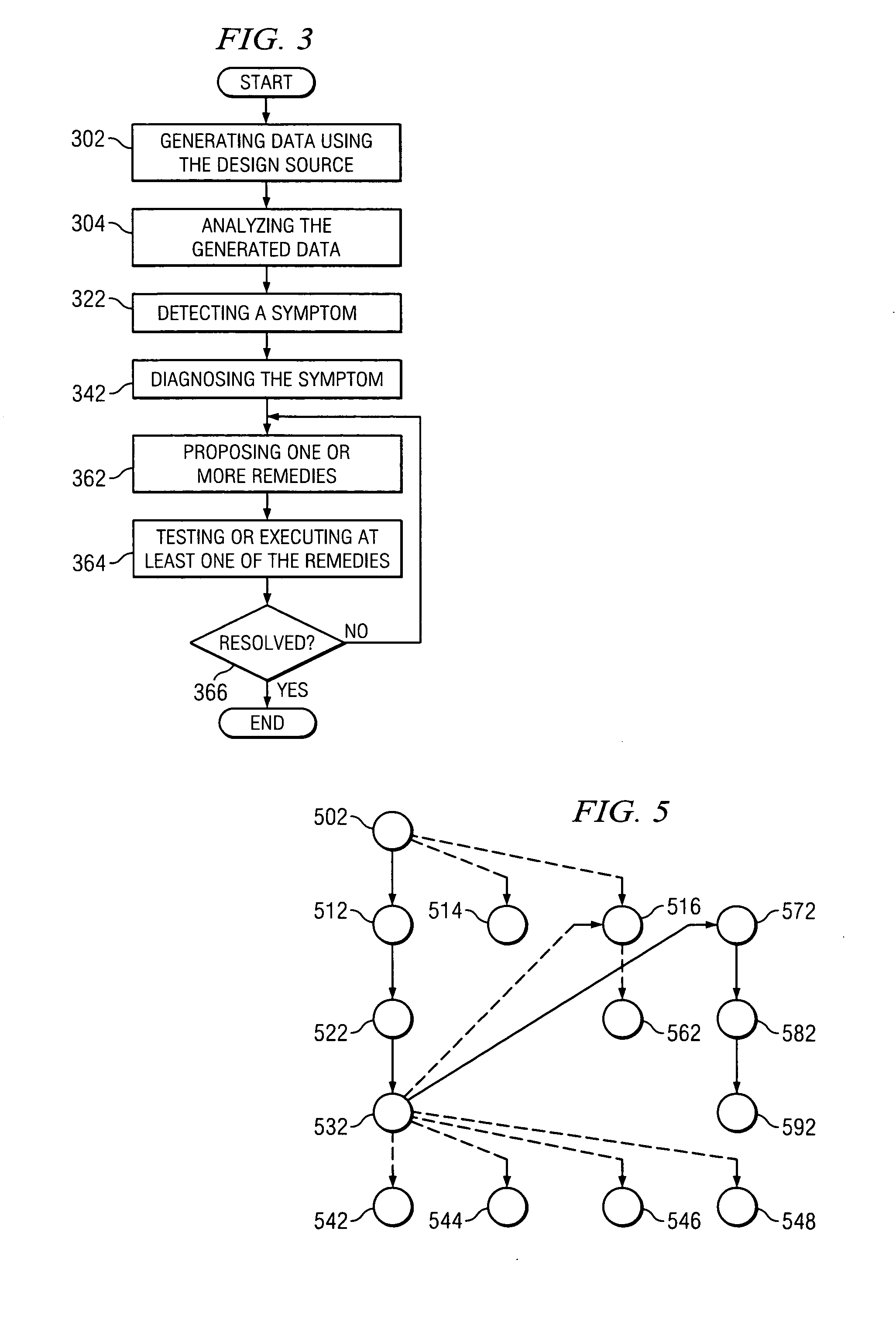
[0032] Reference is now made in detail to the exemplary embodiments of the invention, examples of which are illustrated in the accompanying drawings. Wherever possible, the same reference numbers will be used throughout the drawings to refer to the same or like parts (elements).

[0033] The method and system can mimic the design techniques of expert electronic device designers. Expert designers understand design constructs and what results they are likely to achieve using specific constructs with a given technology. They are also very experienced with the EDA tools. The method and system can use knowledge and observation of both static and dynamic results during and after execution of each design tool or program that defines a design flow. Having used these tools for a number of designs, expert designers are familiar with the tools' behaviors. The method and system can leverage information gleaned from executing a number of designs employing different tools and technologies. The meth...


PUM


Abstract

A system for the automated formation and control and execution of an electronic device design flow is disclosed which can enable more efficient electronic device design methodology with higher quality of results. Such a system as analysis methods, techniques, and tools, a knowledge database, a design database a controller and reasoner, are described.

Description

RELATED APPLICATIONS [0001] This application claims priority under 35 U.S.C. § 119(e) to U.S. Patent Application No. 60 / 427,474, entitled “System and Method for Automated IC Design System” by Bohl et al., filed on Nov. 19, 2002, which is assigned to the current assignee hereof and incorporated herein by reference.FIELD OF THE INVENTION [0002] The invention relates in general to systems and methods for designing electronic devices, and more particularly, to systems and methods for automating the design of electronic devices including electronic semiconductor devices. DESCRIPTION OF THE RELATED ART [0003] Even though Electronic Design Automation (EDA) tools have made considerable progress in automating many of the previously manual design activities, semiconductor process technology and escalating circuit densities combine to make design an increasingly complicated and expensive undertaking. As semiconductor device technology trends toward smaller devices, greater levels of expertise ...

Claims


Application Information

Patent Timeline
IPC IPC(8): G06F17/50
CPCG06F17/50G06F30/00
Inventor BOHL, RICHARD L.ROANE, JEFFREY K.
Owner PROPHICY SEMICON
Why Eureka
Try Eureka