High density hybrid MOSFET device

Inactive Publication Date: 2006-12-07
M MOS SEMICON
View PDF2 Cites 44 Cited by
  • Summary
  • Abstract
  • Description
  • Claims
  • Application Information

AI Technical Summary

Benefits of technology

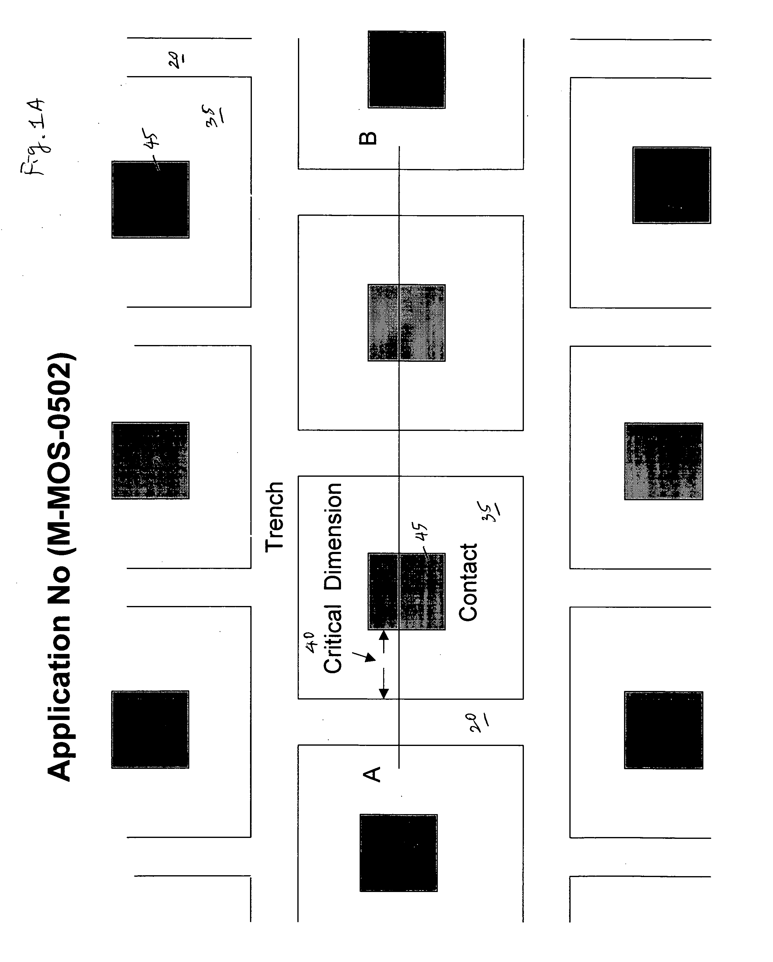
[0008] It is therefore an object of the present invention to provide new and improved semiconductor power device configuration, e.g., a MOSFET device that comprises hybrid cells. The hybrid cells are implemented with closed MOSFET cells and stripe MOSFET cells with the closed MOSFET cells surrounded by trenched gates with a trenched source body contact disposed in the center to comply with the critical dimension requirement for maintaining a minimum d

Problems solved by technology

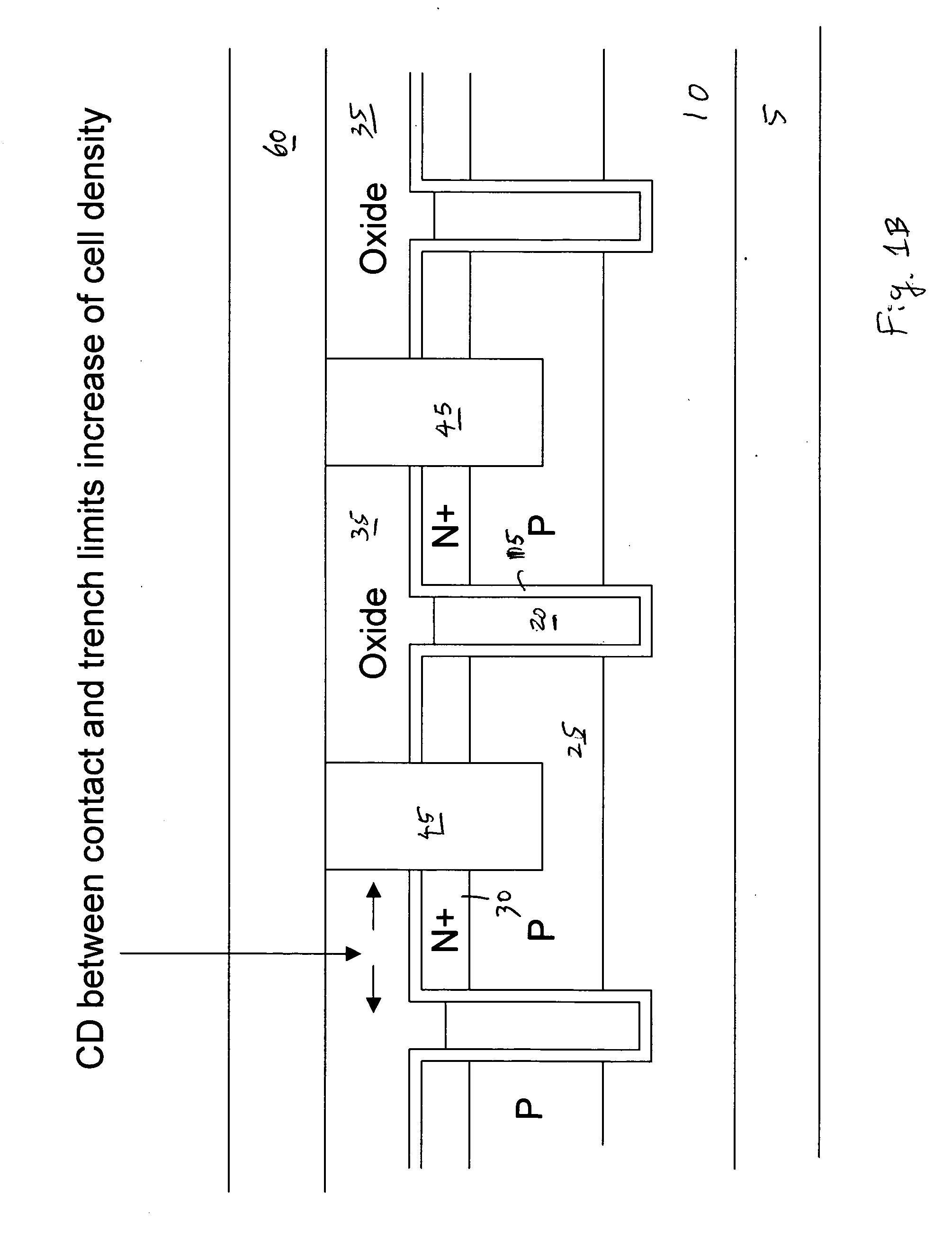
As the cell density of the semiconductor power devices increases, several critical dimensions (CDs) such as the distance between the contact and the trench becomes a limiting factor.
However, the when a greater distance between the trenched gate and the source contact is applied to accommodate potential misa

Method used


Image

  • High density hybrid MOSFET device
  • High density hybrid MOSFET device
  • High density hybrid MOSFET device

Examples


Embodiment Construction

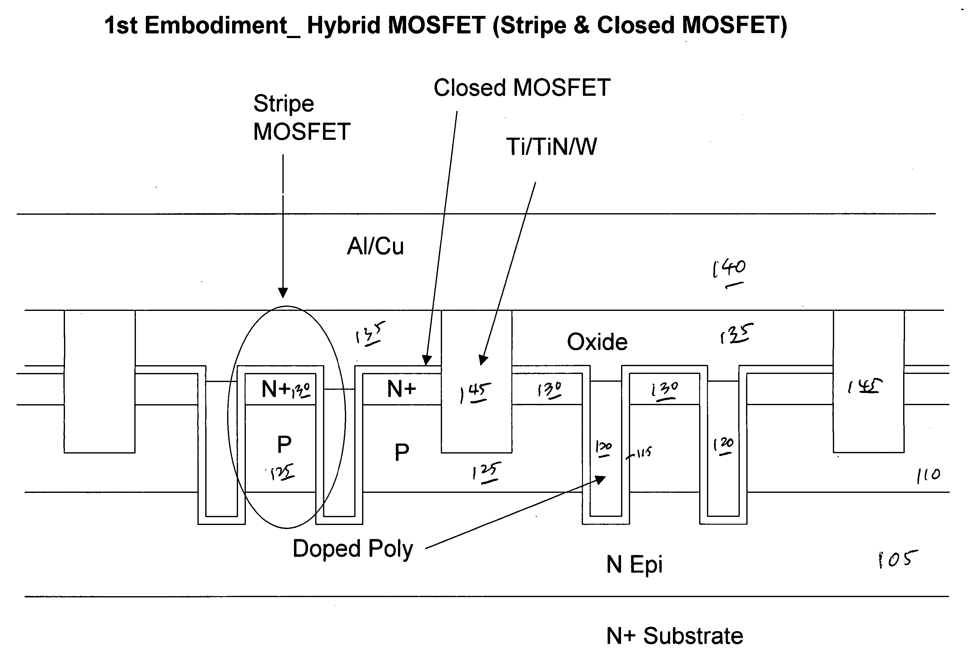
[0020] Please refer to FIGS. 2A to 2B for a first preferred embodiment of this invention where a metal oxide semiconductor field effect transistor (MOSFET) device 100 is supported on a substrate 105 formed with an epitaxial layer 110. The MOSFET device 100 includes a trenched gate 120 disposed in a trench with a gate insulation layer 115 formed over the walls of the trench. A body region 125 that is doped with a dopant of second conductivity type, e.g., P-type dopant, extends between the trenched gates 120. The P-body regions 125 encompassing a source region 130 doped with the dopant of first conductivity, e.g., N+ dopant. The source regions 130 are formed near the top surface of the epitaxial layer surrounding the trenched gates 120. The top surface of the semiconductor substrate extending over the top of the trenched gate, the P body regions 125 and the source regions 130 are covered with a NSG and a BPSG protective layers 135. A source metal layer 140 and gate metal layer (not sh...


PUM


Abstract

A hybrid semiconductor power device that includes a plurality of closed power transistor cells each surrounded by a first and second trenched gates constituting substantially a closed cell and a plurality of stripe cells comprising two substantially parallel trenched gates constituting substantially an elongated stripe cell wherein the closed cells and stripe cells constituting neighboring cells sharing trenched gates disposed thereinbetween as common boundary trenched gates. The closed MOSFET cell further includes a source contact disposed substantially at a center portion of the closed cell wherein the trenched gates are maintained a critical distance (CD) away from the source contact.

Description

[0001] This Patent application is a Continuation in Part (CIP) Application of a co-pending application Ser. No. 11 / 147,075 filed by a common Inventor of this Application on Jun. 6, 2005 with a Serial Number. The Disclosures made in that Application is hereby incorporated by reference.BACKGROUND OF THE INVENTION [0002] 1. Field of the Invention [0003] This invention relates generally to the cell structure, device configuration and fabrication process of power semiconductor devices. More particularly, this invention relates to a novel and improved cell structure, device configuration and improved process for fabricating a trenched semiconductor power device with improved increased cell density by reducing a gate to source contact critical dimension (CD) requirement. [0004] 2. Description of the Related Art [0005] As the cell density of the semiconductor power devices increases, several critical dimensions (CDs) such as the distance between the contact and the trench becomes a limiting...

Claims


Application Information

Patent Timeline
IPC IPC(8): H01L29/78H01L21/336
CPCH01L24/26H01L24/40H01L24/45H01L24/49H01L24/83H01L24/85H01L29/41766H01L29/456H01L29/66727H01L29/66734H01L29/7813H01L2224/05624H01L2224/05655H01L2224/45015H01L2224/45124H01L2224/45144H01L2224/48247H01L2224/48472H01L2224/48624H01L2224/48655H01L2224/48724H01L2224/48755H01L2224/4903H01L2224/49051H01L2224/49111H01L2224/83801H01L2224/85H01L2924/01005H01L2924/01013H01L2924/01014H01L2924/01015H01L2924/01018H01L2924/01022H01L2924/01027H01L2924/01028H01L2924/01029H01L2924/01042H01L2924/01047H01L2924/0105H01L2924/01074H01L2924/01079H01L2924/04941H01L2924/13091H01L2924/20755H01L2924/2076H01L2924/30105H01L2924/01033H01L2924/1306H01L2924/00014H01L2924/00H01L29/7828H01L29/0696H01L24/48H01L2224/73221
Inventor HSHIEH, FWU-IUAN
Owner M MOS SEMICON
Why Eureka
Try Eureka