Semiconductor device comprising an integrated circuit

Inactive Publication Date: 2006-12-07
SEIKO EPSON CORP
View PDF6 Cites 10 Cited by
  • Summary
  • Abstract
  • Description
  • Claims
  • Application Information

AI Technical Summary

Problems solved by technology

Miniaturization of the components of the integrated circuits is a critical issue i.e. it is essential to pack the greatest possible amount of components in a microchip.
It is however difficult to reduce the size of the passive components to a level being comparable to the size reduction achieved for transistors so that the presence of such passive components limits that layout space available for designing the integrated circuits on the microchips having the above described typical structure.
This conventional structure of microchip

Method used


Image

  • Semiconductor device comprising an integrated circuit
  • Semiconductor device comprising an integrated circuit
  • Semiconductor device comprising an integrated circuit

Examples


first embodiment

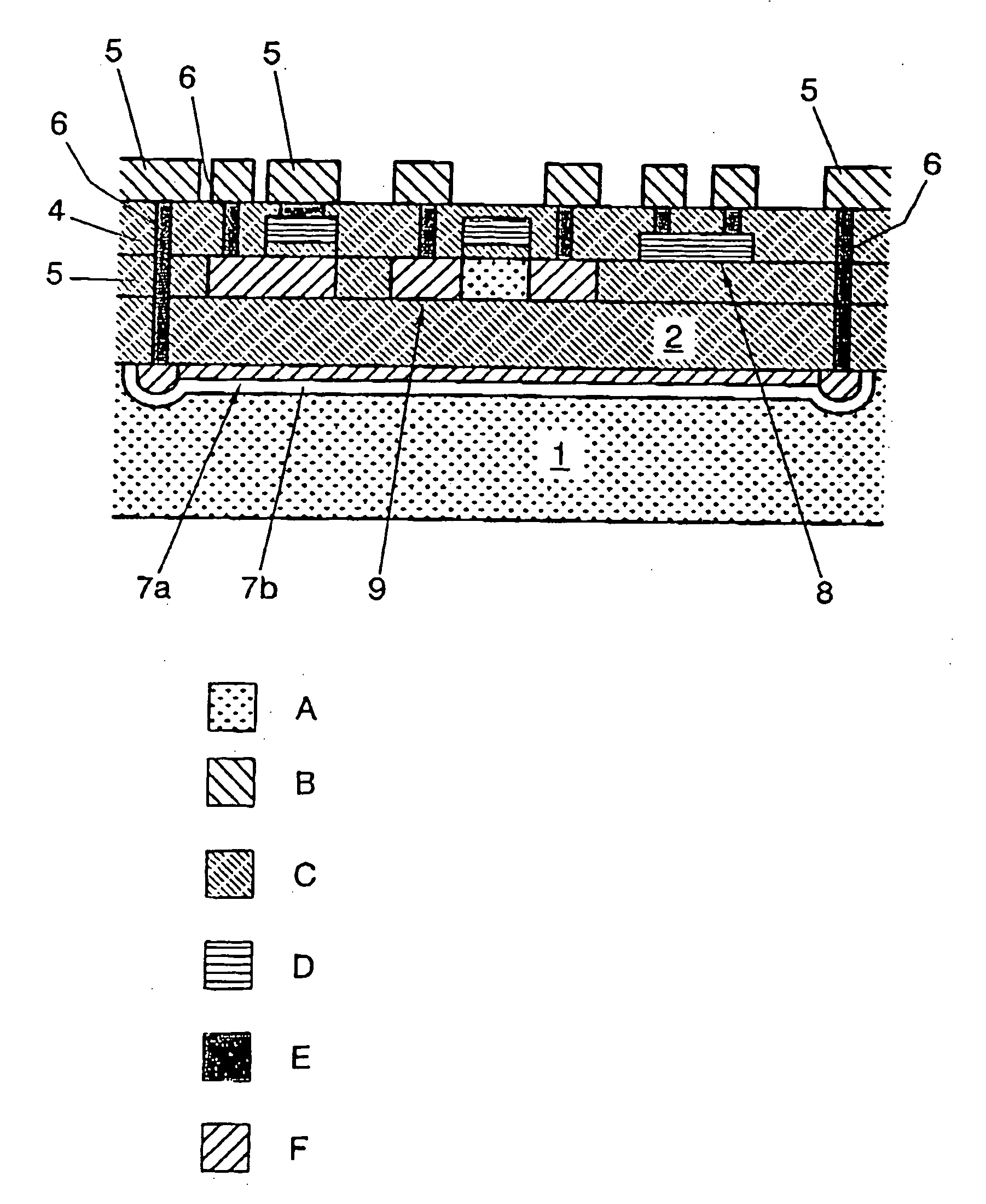
[0041]FIG. 2 is a partial schematic sectional view of the a semiconductor device in accordance with a first embodiment;

second embodiment

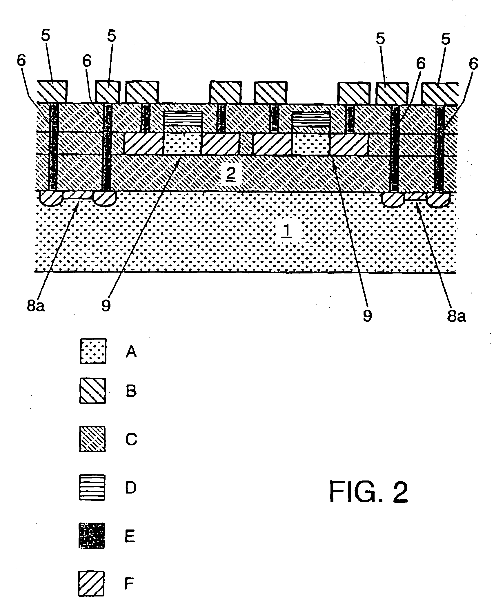
[0042]FIG. 3 is a partial schematic sectional view of the a semiconductor device in accordance with a second embodiment;

third embodiment

[0043]FIG. 4 is a partial schematic sectional view of the a semiconductor device in accordance with a

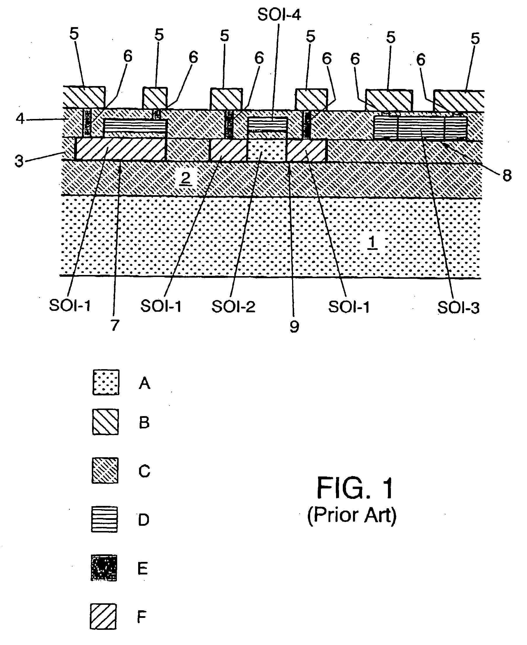
[0044] In these figures, there appear reference signs having the following meanings: [0045]1 bottom substrate [0046]2 BOX layer [0047]3 dielectric intermediate insulating layer [0048]4 dielectric top insulating layer [0049]5 top metal connecting elements [0050]6 via hole [0051]7 capacitor [0052]7a capacitor implanted below BOX layer (AC decoupling capacitor) [0053]7b depletion layer [0054]8 resistor [0055]8a resistor below BOX layer [0056]9 transistor [0057] SOI-1, SOI-2, SOI-3, SOI-4 silicon on insulator (“SOI”) layer portions

[0058] In the figures, elements drawn with the same pattern are of the same type of basic material, namely [0059] A p-semiconductor [0060] B conductive metal of top connecting elements [0061] C silicon dioxide [0062] D polysilicon [0063] E conductive metal in via holes [0064] F n-semiconductor


PUM


Abstract

A semiconductor device with a plurality of passive components (7,7a,8,8a) comprising a bottom substrate (1), a buried oxide layer (2) on a portion of the top surface of the bottom substrate (1), an dielectric intermediate insulating layer (3) on a portion of the buried oxide layer (2), a dielectric top insulating layer (4), and at least one implanted passive component (7a,8a) of a semiconductor material implanted under the buried oxide layer (2) within the top surface portion of the bottom substrate (1), the implanted semiconductor material having a material polarity being opposite to the bottom substrate polarity. When the implanted passive component (7a) is an AC decoupling capacitor (7a), the bottom and side portions of the implanted semiconductor material are surrounded by a depletion layer (7b) of a semiconductor material implanted between said bottom substrate (1) and said implanted semiconductor material.

Description

TECHNICAL FIELD OF THE INVENTION [0001] The present invention lies within the field of semiconductor devices comprising integrated circuits. More particularly, the invention pertains to the sector of semiconductor devices comprising passive components such as resistors, inductors, capacitors etc. being part of electric circuits integrated in semiconductor devices. BACKGROUND OF THE INVENTION [0002] Semiconductor devices comprising integrated circuits like microchips are of widespread application in electronics such as computer hardware. Miniaturization of the components of the integrated circuits is a critical issue i.e. it is essential to pack the greatest possible amount of components in a microchip. Typical components are transistors, and so-called passive components such as resistors, inductors and capacitors. [0003] A typical conventional structure of semiconductor devices is comprised of a bottom substrate having a top surface and a bottom substrate polarity, a silicon on insu...

Claims


Application Information

Patent Timeline
IPC IPC(8): H01L27/12
CPCH01L21/8252H01L27/1203H01L27/0605H01L21/84
Inventor TANAKA, KAZUAKI
Owner SEIKO EPSON CORP
Why Eureka
Try Eureka