Phase-change optical recording medium
a technology of optical recording medium and phase change, which is applied in the field of phase change optical recording medium, can solve the problems of information in a certain track deteriorating, so-called cross-erase problems, and errors in the stage of converting obtained signals into digital data
- Summary
- Abstract
- Description
- Claims
- Application Information
AI Technical Summary
Benefits of technology
Problems solved by technology
Method used
Image
Examples
example 1
[0049] A polycarbonate (PC) substrate having a thickness of 0.59 mm, which was prepared by injection molding, was used as a substrate. Since grooves were formed on the substrate at a groove pitch of 0.68 μm, the track pitch was 0.34 μm in land-groove recording.
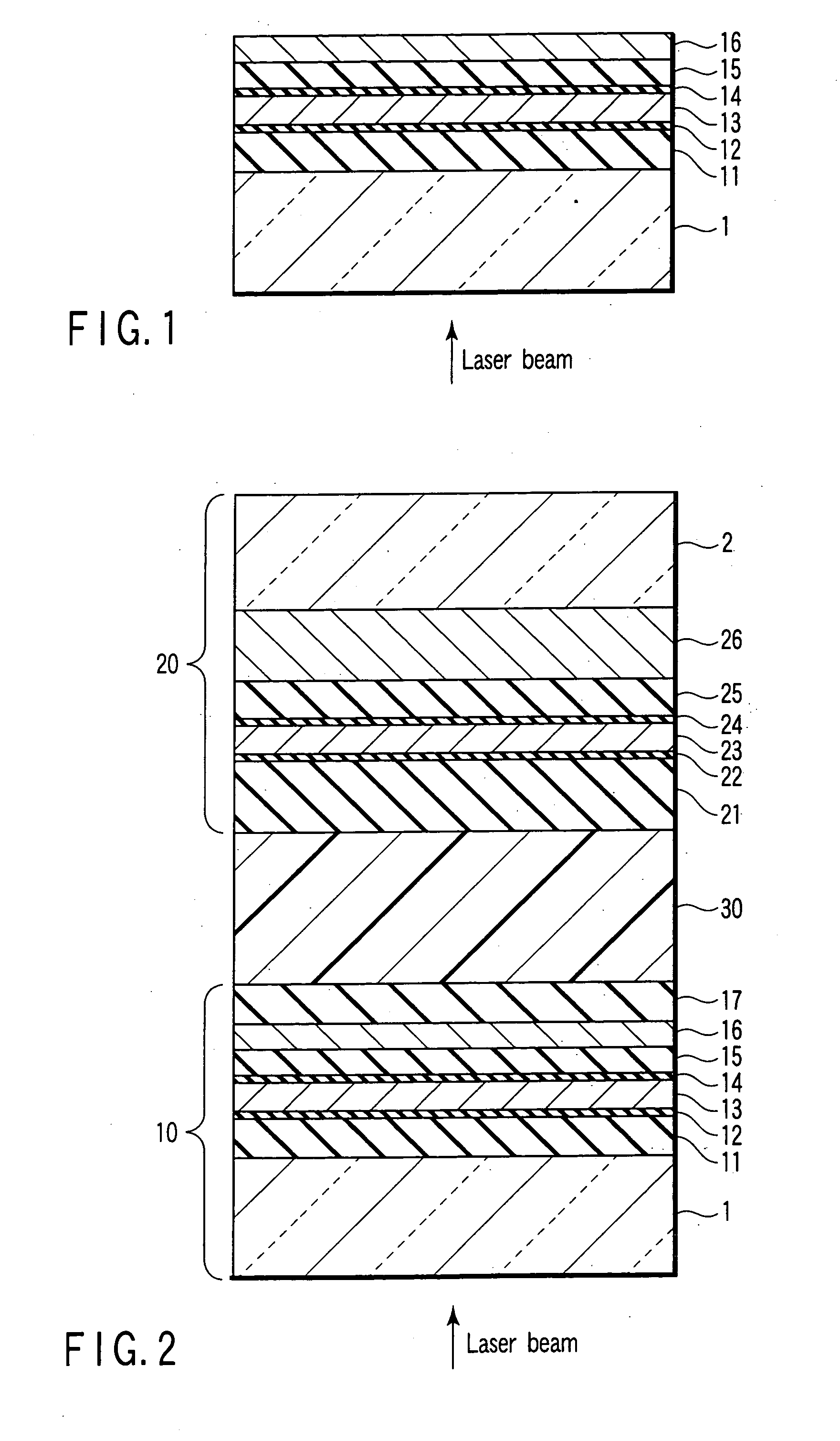
[0050] An L0 information layer was prepared by forming various films on the surface of a first substrate by sputtering, and an L1 information layer was prepared by forming various films on the surface of a second substrate by sputtering. The films are formed in different deposition chambers using the sputtering apparatus with multi process chambers.
[0051] To be more specific, a ZnS:SiO2 film (first interference film), a lower interface film, a phase-change optical recording film, an upper interface film, a ZnS:SiO2 film (second interference film), an Ag alloy film (reflective film), and a ZnS:SiO2 film (thermal diffusion film) were formed successively on the surface of the first substrate in the order mentioned so as to prep...
examples 2 to 9
[0065] Discs of the construction equal to that of Example 1 were prepared by using various interface films. Specifically, interface films formed of HfSi0.4O4C0.5, HfSi0.1O2.5C0.1, HfSi0.2O3.5C0.01, HfSi0.15O2.8C0.001, HfSi0.18O3.1C0.0001, HfSi0.18O3C0.1, HfSi0.17O3.2C0.01, and HfSi1.6O2.9C0.0001 were used. Tests equal those applied in Example 1 were applied to the manufactured discs. The results of the tests are shown in Table 2. As is apparent from Table 2, good characteristics were obtained in each of Examples 2 to 9.
TABLE 2BeforeAfterenvironmentalAfter OWenvironmentalExtinctiontesttesttestInterface filmcoefficientCNR[dB]SbERSbERSbERExample 1HfSi0.1O1.8C0.001054.62.0 × 10−52.4 × 10−52.9 × 10−5Example 2HfSi0.4O4C0.51.0 × 10−453.21.9 × 10−52.5 × 10−52.8 × 10−5Example 3HfSi0.1O2.5C0.11.1 × 10−553.82.4 × 10−52.8 × 10−52.9 × 10−5Example 4HfSi0.2O3.5C0.01053.62.2 × 10−52.6 × 10−52.8 × 10−5Example 5HfSi0.15O2.8C0.001052.12.4 × 10−52.9 × 10−52.9 × 10−5Example 6HfSi0.18O3.1C0.0001053.91....
examples 10 to 50
[0066] Discs of the construction equal to that in Example 1 were prepared by changing the material of the interface film. The materials used for the interface films were HfSiOCN, HfSiON, ZrSiOC, ZrSiOCN, TiSiOC, TiSiON, NbSiOC, NbSiOCN, AlSiOC, AlSiOCN, ZnSiOC, ZnSiOCN, YSiOC, YSiON, LaSiOC, LaSiOCN, CeSiOC, CeSiON, PrSiOC, PrSiON, SmSiOC, SmSiOCN, EuSiOC, EuSiON, GdSiOC, GdSiOCN, TbSiOC, TbSiOCN, DySiOC, DySiON, HoSiOC, HoSiOCN, ErSiOC, ErSiON, TmSiOC, TmSiOCN, YbSiOC, YbSiOCN, LuSiOC, and LuSiOCN. Incidentally, the composition of all the interface films was optimized so as to lower the extinction coefficient. Tests equal to those applied in Example 1 were applied to the discs thus manufactured. The results of the tests are shown in Tables 3 to 6. As is apparent from these tables, the disc prepared in any of these Examples was satisfactory in CNR and SbER;
PUM
| Property | Measurement | Unit |
|---|---|---|
| transmittance | aaaaa | aaaaa |
| thickness | aaaaa | aaaaa |
| wavelength | aaaaa | aaaaa |
Abstract
Description
Claims
Application Information
