Semiconductor device and method of producing same

a technology of semiconductors and semiconductors, applied in the direction of transistors, television systems, radio control devices, etc., can solve the problem that the structure of the surface channel type mos transistor designed based on the constant electric field scaling rule is not suitable for the source-follower circuit, and achieves the reduction of noise, the improvement of the linearity characteristic of the source, and the reduction of the variation of the threshold value

Inactive Publication Date: 2006-12-07
SONY SEMICON SOLUTIONS CORP
View PDF37 Cites 32 Cited by
  • Summary
  • Abstract
  • Description
  • Claims
  • Application Information

AI Technical Summary

Benefits of technology

[0022] According to an embodiment of the present invention, a semiconductor device suitable for application to a source-follower circuit can be realized. Namely, when applying the semiconductor device of an embodiment of the present invention to a source-follower circuit, the linearity characteristic of the source can be improved. Further, in the semiconductor device of an embodiment of the present invention, an effect of reduction of noise

Problems solved by technology

As described above, a surface channel type MOS transistor designed based on the constant electric field scaling rule does not have a structure suitable for a source-follower circuit.
Further, when amplifying a signal in a source-follower circuit, due to the trap

Method used


Image

  • Semiconductor device and method of producing same
  • Semiconductor device and method of producing same
  • Semiconductor device and method of producing same

Examples


Embodiment Construction

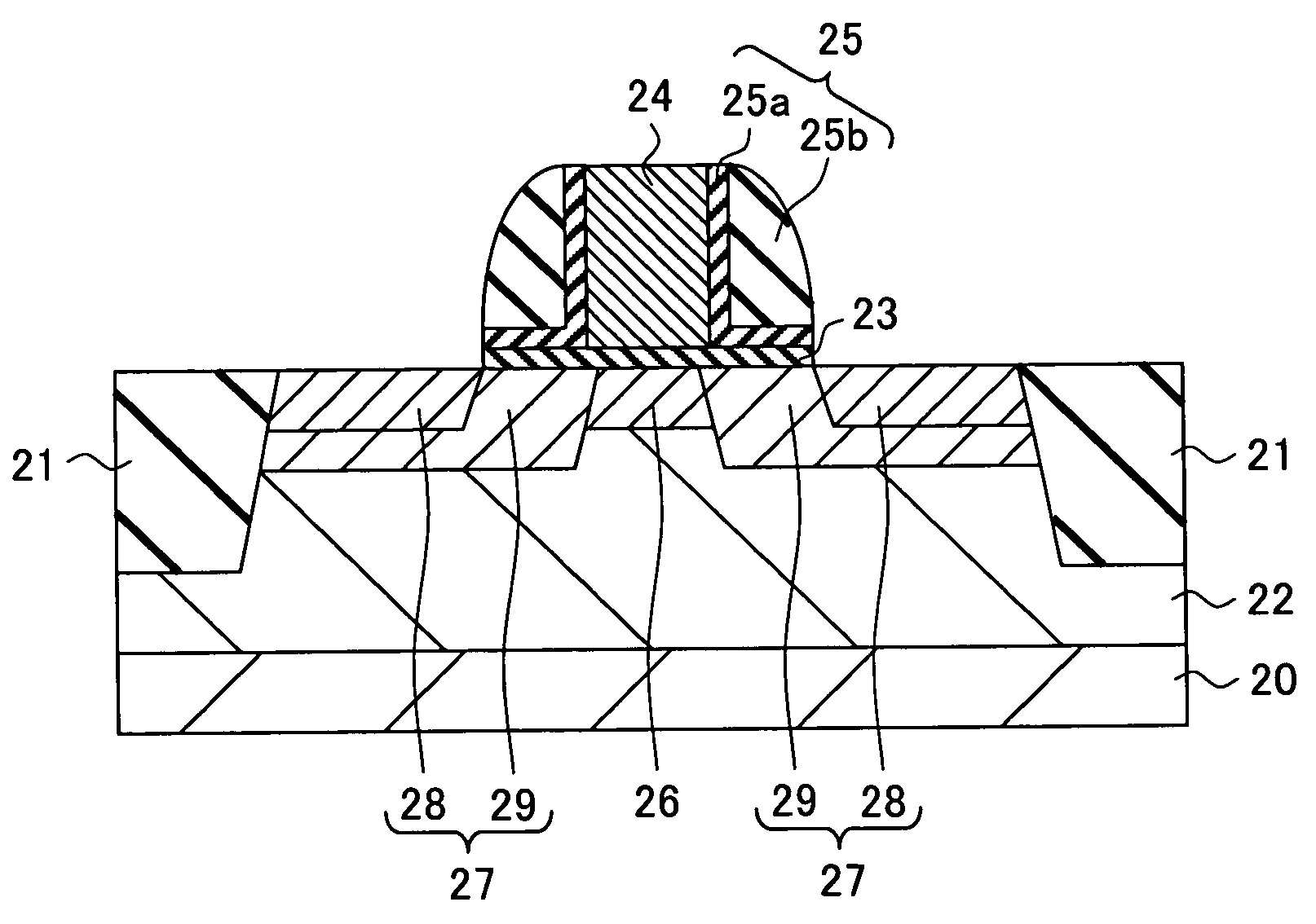
[0034] Below, a semiconductor device of an embodiment of the present invention will be explained with reference to the drawings. In the present embodiment, an example of applying the semiconductor device of the present invention to an MOS type image sensor will be explained.

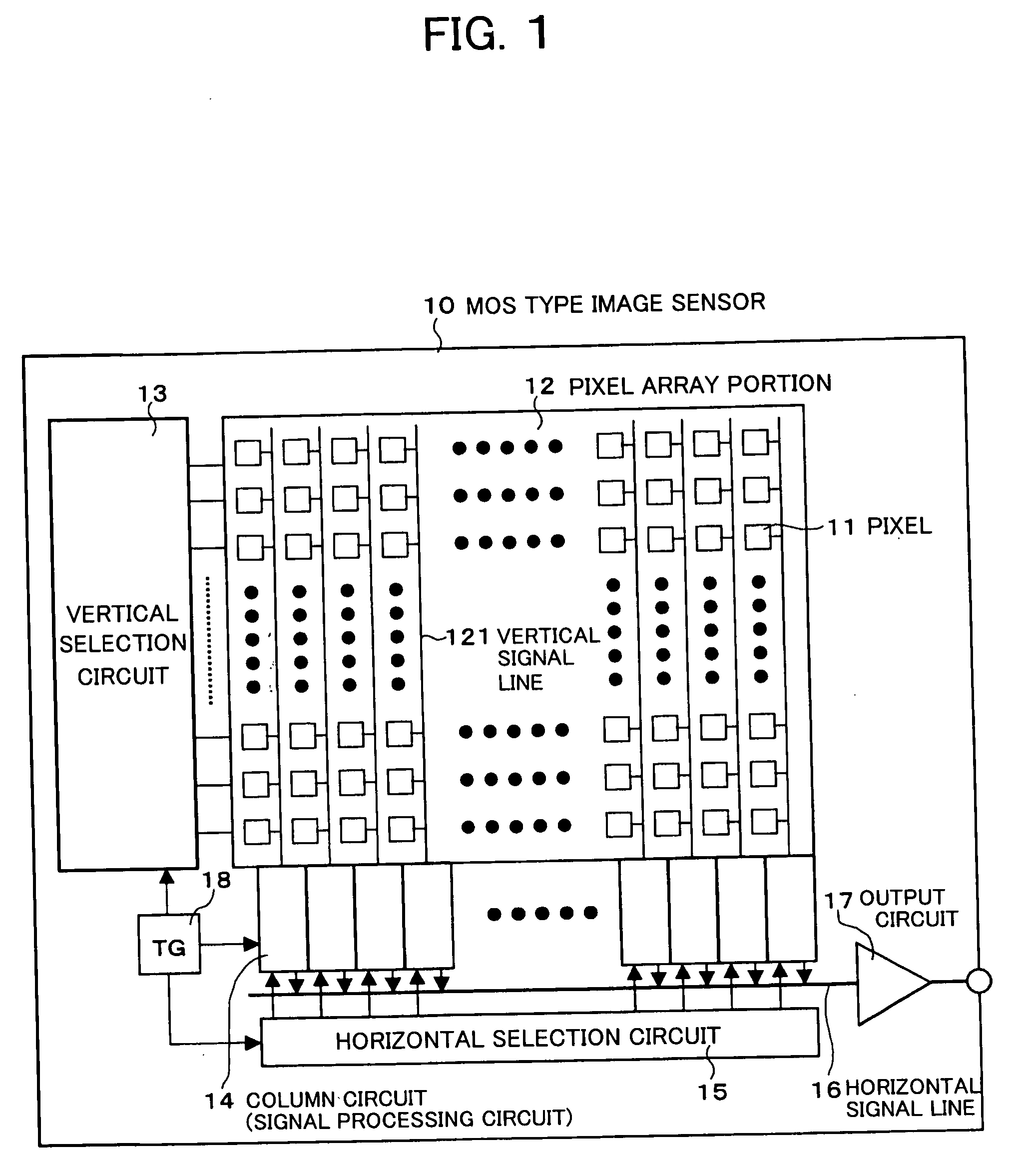
[0035]FIG. 1 is a block diagram illustrating an example of the configuration of an amplification type solid-state imaging device, for example, an MOS type image sensor, to which the present invention is applied.

[0036] A MOS type image sensor 10 has picture elements 11 including for example photodiodes as a photo-electric conversion element, a pixel array portion 12 including the picture elements 11 arranged two-dimensionally in a matrix, a vertical selection circuit 13, signal processing circuits including column circuits 14, a horizontal selection circuit 15, a horizontal signal line 16, an output circuit 17, and a timing generator (TG) 18.

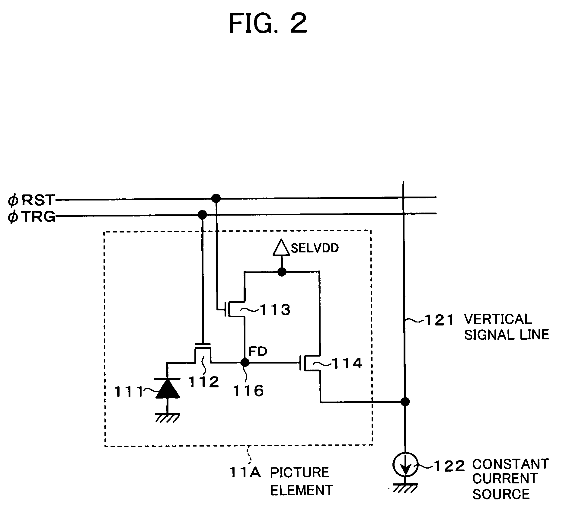
[0037] In the pixel array portion 12, a vertical signal line 121 is ar...


PUM


Abstract

A semiconductor device suitable for a source-follower circuit, provided with a gate electrode formed on a semiconductor substrate via a gate insulation film, a first conductivity type layer formed in the semiconductor substrate under a conductive portion of the gate electrode and containing a first conductivity type impurity, first source/drain regions of the first conductivity type impurity formed in the semiconductor substrate and extended from edge portions of the gate electrode, and second source/drain regions having a first conductivity type impurity concentration lower than that in the first source/drain regions and formed adjoining the gate insulation film and the first source/drain regions in the semiconductor substrate so as to overlap portions of the conductive portion of the gate electrode.

Description

CROSS REFERENCE TO RELATED APPLICATION [0001] The present invention contains subject matter related to Japanese Patent Application No. 2005-141248 filed in the Japan Patent Office on May 13, 2005, the entire contents of which being incorporated herein by reference. BACKGROUND OF THE INVENTION [0002] 1. Field of Invention [0003] The present invention relates to a semiconductor device and a method of producing the same, more particularly relates to a semiconductor device applied to for example a source-follower circuit and a method of producing the same. [0004] 2. Description of the Related Art [0005] In recent years, as a solid-state imaging device mounted on a camera-function mobile phone, a personal digital assistant (PDA), or other mobile device, for example from the viewpoint of the power consumption, a MOS type image sensor requiring a lower power voltage in comparison with a CCD image sensor is frequently used. [0006] Japanese Patent Publication (A) No. 2002-51263 for example d...

Claims


Application Information

Patent Timeline
IPC IPC(8): H01L21/00H01L21/336H01L23/58H01L27/146H01L29/78H04N5/335H04N5/369H04N5/374
CPCH01L29/6656H01L29/6659Y10S438/945H04N5/3741H01L29/7838H01L29/7833H04N25/766
Inventor ITONAGA, KAZUICHIRO
Owner SONY SEMICON SOLUTIONS CORP
Why Eureka
Try Eureka